4 layers

 blurbler2/powerboard
Tree Sentinel powerboard: standalone TPS62842 3.3 V buck module for 4xAA NiMH, breadboard format (KiCad 10)
Powerboard v1 is an open-source printed circuit board by blurbler2, from the blurbler2/powerboard repository on GitHub. It is a 2-layer board of 16 × 45.7 mm with 25 parts on 14 nets, routed with 70 tracks and 16 vias.
It is built around the TPS62842DGRR, AO3400A and AO3401A, with the OS102011MA1QN1 and SS14 among its other parts. Its parts include 6 capacitors, 5 resistors, 3 connectors, 2 transistors and 1 IC. It belongs with the power boards of this library.


A small 3.3 V supply module for battery-powered microcontroller projects: 4x AA NiMH in, regulated 3.3 V out, with an ultra-low quiescent current buck converter (TI TPS62842, 60 nA Iq), a switchable battery-voltage divider for an MCU ADC, a jumper for current measurement and test points. Breadboard format with two 1x04 pin headers 12.7 mm apart, like olmBoard (which uses the TPS62840 from the same family).
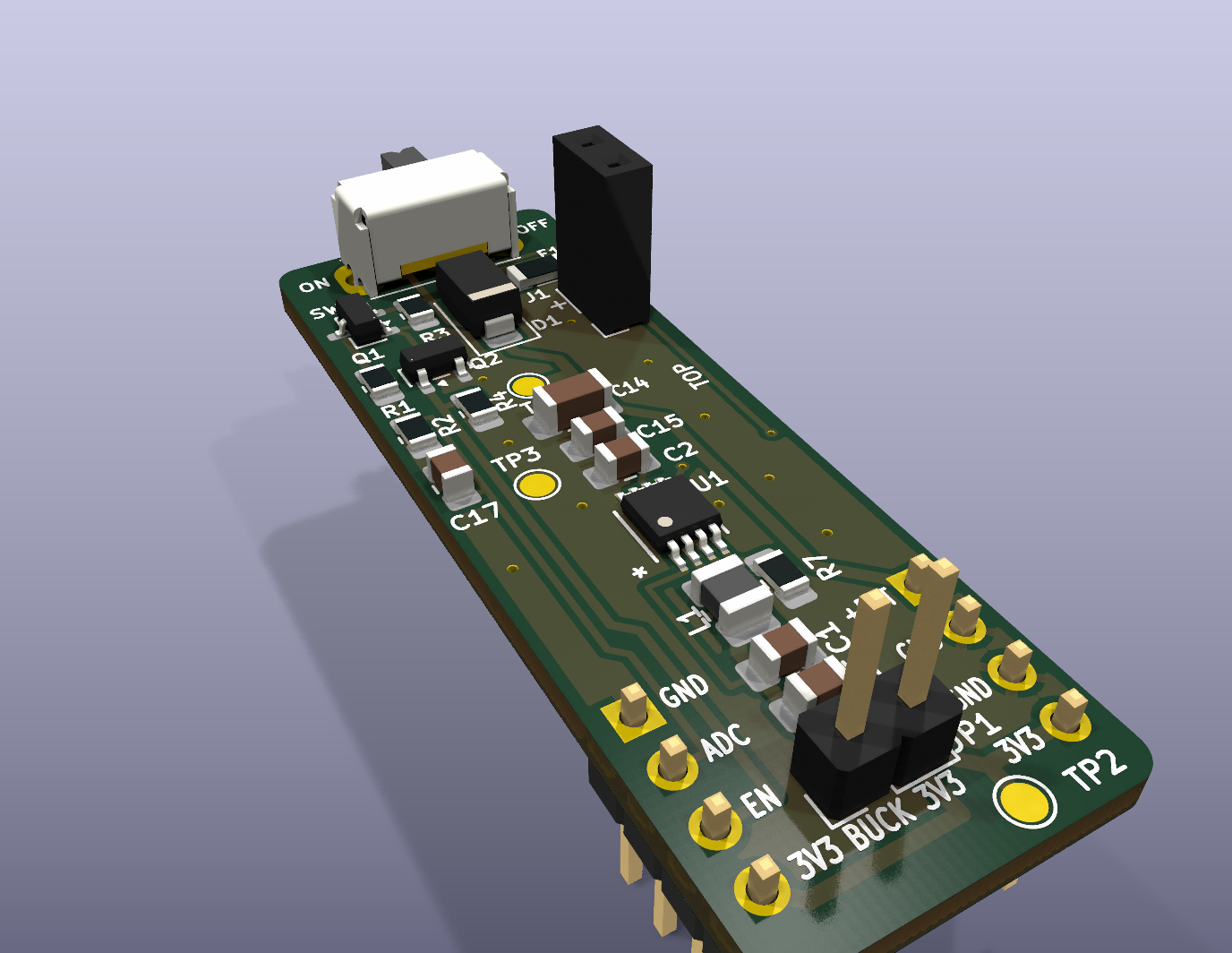
| Input | 4x AA NiMH, 4.8 ... 5.6 V (converter accepts 1.8 ... 6.5 V) |
| Output | 3.3 V (set by R7 = 52.3 kΩ 1 %) |
| Output current | up to 750 mA (converter limit); F1 holds 500 mA from the battery, which is about 600 mA at 3.3 V even with nearly empty cells. SW1 carries no load current (see SW1) |
| Quiescent current | ON: 60 nA (TPS62842) + MOSFET leakage, the battery divider draws nothing while it is off. OFF: converter shut down, 25 nA typ. (datasheet max 300 nA) + leakage |
| Protection | 500 mA polyfuse F1, reverse-polarity Schottky diode D1 (SS14) |
| Board | 16.0 x 45.72 mm, 2 layers, 1.6 mm, KiCad 10 |
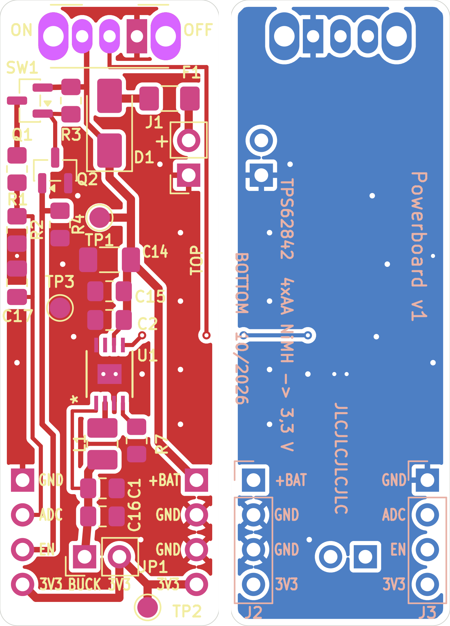
Top view, switch at the top edge:
     ON <-- SW1 --> OFF  (actuator sticks out over the edge)
   Q1 R3              D1        F1
   R1 Q2                        J1  (battery: + upper pin, - square pad)
   R2 R4   TP1 (+BATT)
   C17     C14 C15 C2
   TP3 (GND)    U1                  TOP
                L1 R7
  J3 ●  GND     C1 C16       +BAT  ● J2
     ●  ADC                   GND  ●
     ●  EN      JP1 [BUCK|3V3] GND  ●
     ●  3V3                   3V3  ●
TP2 (+3V3)2-pin socket, 2.54 mm pitch, for the plug of a 4x AA holder.
| J1 pin | Silkscreen | Connect |
|---|---|---|
| 1 | square pad | battery − (black) |
| 2 | + | battery + (red) |
D1 blocks a reversed battery, so a wrong plug does no harm (the board just stays off).
Mounted from the bottom: plastic under the board, long pins down into the breadboard. Pin 1 is on the switch side. The labels are printed next to the pins on both sides of the board.
| Pin | J3 (left, SIG) | J2 (right, PWR) |
|---|---|---|
| 1 | GND | +BATT (battery after F1 and D1, live even when SW1 is OFF) |
| 2 | ADC (battery voltage / 2, only while EN is high) | GND |
| 3 | EN (enable battery measurement, 3.3 V logic input) | GND |
| 4 | +3V3 | +3V3 |
+3V3 on J2.4 and J3.4 is the same rail, after the current jumper JP1. All GND pins are the same.
J3 EN only switches the battery divider; it has nothing to do with SW1.
SW1 is a C&K OS102011MA1Q, a right-angle (side-actuated) SPDT slide switch, through-hole. The footprint looks big because of its two large oval pads: they are the soldered legs of the metal frame that hold the switch mechanically and carry no signal. The three small pads in the middle are the contacts.
SW1 does not sit in the battery line. It drives the enable pin of the converter (net BUCK_EN):
| Slider position | Silkscreen | Contacts (C&K switch function) | Result |
|---|---|---|---|
| left | ON | middle pin to left pin (2-3) → EN = +BATT | converter runs, +3V3 on |
| right | OFF | middle pin to right pin (1-2) → EN = GND | converter shut down (25 nA typ.), +3V3 discharged to 0 V |
ON / OFF labels are printed at the matching ends of the switch.| Powerboard | Nucleo |
|---|---|
| J3.1 GND | GND |
| J3.2 ADC | any ADC input pin (Arduino header A0 ... A5) |
| J3.3 EN | any free GPIO, push-pull output |
| J3.4 +3V3 | 3V3, only if the Nucleo is not powered over USB at the same time |
If the Nucleo runs from USB, connect only GND, ADC and EN; never tie two 3.3 V supplies together.
The TPS62842 needs 3 ... 40 µF effective capacitance on its output (datasheet, COUT). C1 gives about 5 µF at 3.3 V; everything the load adds on +3V3 counts too, so keep the load's own capacitance below about 30 µF.
R1/R2 (100 kΩ / 100 kΩ, 1 %) divide the battery voltage by two. Q1 (AO3401A, P-channel) switches the divider on and off at the battery side, Q2 (AO3400A, N-channel) lets a 3.3 V GPIO drive Q1.
| EN | State | Current |
|---|---|---|
| high (3.3 V) | Q2 on → Q1 on → divider on, ADC = VBAT / 2 | ≈ 37 µA (28 µA divider, 5.6 µA R3, 3.3 µA R4) |
| low or open | R4 keeps Q2 off, R3 keeps Q1 off → divider off, ADC = 0 V | MOSFET leakage only (nA) |
One measurement (100 ms at 37 µA) costs about 4 µC, roughly 1 nA on average when measuring once per hour. The divider is off while the MCU is in reset or the pin is floating, so it never drains the battery by accident. While it is off the ADC pin sees 0 V, never more than the MCU supply.
Measurement sequence:
Example (STM32 HAL, pin names are placeholders):
HAL_GPIO_WritePin(MEAS_EN_GPIO_Port, MEAS_EN_Pin, GPIO_PIN_SET);
HAL_Delay(100);                                   /* C17 settling, >= 65 ms */
HAL_ADC_Start(&hadc1);
HAL_ADC_PollForConversion(&hadc1, 10);
uint32_t raw = HAL_ADC_GetValue(&hadc1);
HAL_GPIO_WritePin(MEAS_EN_GPIO_Port, MEAS_EN_Pin, GPIO_PIN_RESET);
float vbat = 2.0f * raw * 3.3f / 4095.0f; /* 12 bit, VREF = 3.3 V */JP1 is a 2-pin header with a jumper cap between the converter output and the +3V3 rail. It is not a power connector and has no GND pin.
| JP1 pin | Silkscreen | Net |
|---|---|---|
| 1 (square pad) | BUCK | converter output (U1 / L1 / C1) |
| 2 | 3V3 | +3V3 rail (J2.4, J3.4, TP2) |
The labels are on the top side, under the two pins.
BUCK, black probe (COM) on 3V3.
The meter then shows everything drawn from +3V3 through the headers.SMD pads, 1.5 mm, for probe tips or small clips.
| TP | Net | Where |
|---|---|---|
| TP1 | +BATT (battery after F1 and D1) | below D1, next to Q2 |
| TP2 | +3V3 (after JP1) | bottom edge, right of JP1 |
| TP3 | GND | left side, next to C15 / C2 |
Battery voltage: TP1 against TP3. Output voltage: TP2 against TP3.
Upload powerboard-hw/powerboard-v1/fabrication/powerboard-v1-gerbers.zip (Gerbers + Excellon drill).
| Option | Setting |
|---|---|
| Layers | 2 |
| Dimensions | 16 x 45.72 mm (detected from the outline) |
| Material / thickness | FR-4, 1.6 mm |
| Outer copper | 1 oz |
| Surface finish | HASL lead-free; ENIG if you want flatter pads for U1 |
| Via covering | Tented (the files tent all vias) |
| Mark on PCB | "Specify a location": the order number goes on the JLCJLCJLCJLC text on the bottom |
| Everything else | default |
The design stays inside JLCPCB's standard 2-layer capabilities: tracks ≥ 0.25 mm,
clearance ≥ 0.2 mm, smallest hole 0.3 mm with a 0.6 mm via pad, copper-to-edge 0.5 mm,
silkscreen text 0.8 mm high with 0.15 mm stroke. This is a bare-PCB order; the parts come from
bom/powerboard-v1-bom.csv (JLCPCB assembly would additionally need LCSC part numbers).
Hand-solder footprints throughout, except U1:
First power-up, without a load:
OFF (slider right), jumper cap on JP1, batteries in.ON (slider left): TP2–TP3 = 3.3 V.Default 0.4 mm, Versorgung (supply) 0.6 mm; copper-to-edge 0.5 mmpowerboard/
├── README.md
├── powerboard-docs/ renders: 3D, top, bottom, layout, schematic
└── powerboard-hw/
├── powerboard-lib/ project library: TPS62842DGRR symbol, DGR footprint, STEP model
└── powerboard-v1/ KiCad 10 project
├── powerboard-v1.kicad_pro / .kicad_sch / .kicad_pcb / .kicad_dru
├── sym-lib-table, fp-lib-table (only ${KIPRJMOD}-relative paths)
├── schematic/ schematic PDF
├── bom/ BOM (CSV, grouped by value and footprint)
└── fabrication/ Gerbers, Excellon drill, position file, gerber zipOnly the KiCad standard libraries are needed besides this folder.
From powerboard-hw/powerboard-v1/:
kicad-cli pcb export gerbers -l F.Cu,B.Cu,F.Paste,B.Paste,F.Silkscreen,B.Silkscreen,F.Mask,B.Mask,Edge.Cuts --use-drill-file-origin --subtract-soldermask -o fabrication/gerbers/ powerboard-v1.kicad_pcb
kicad-cli pcb export drill --drill-origin plot --excellon-separate-th --generate-map --map-format gerberx2 -o fabrication/gerbers/ powerboard-v1.kicad_pcb
kicad-cli pcb export pos --side both --format csv --units mm --use-drill-file-origin -o fabrication/powerboard-v1-pos.csv powerboard-v1.kicad_pcb
kicad-cli sch export bom --fields 'Reference,Value,Footprint,${QUANTITY},Datasheet,Description' --labels 'Refs,Value,Footprint,Qty,Datasheet,Description' --group-by 'Value,Footprint' -o bom/powerboard-v1-bom.csv powerboard-v1.kicad_sch
kicad-cli sch export pdf -o schematic/powerboard-v1.pdf powerboard-v1.kicad_schv1, not manufactured or tested yet.
| Qty | Value | Footprint | References |
|---|---|---|---|
| 2 | 100k | Resistor_SMD:R_0805_2012Metric_Pad1.20x1.40mm_HandSolder | R1, R2 |
| 2 | 100nF | Capacitor_SMD:C_0805_2012Metric_Pad1.18x1.45mm_HandSolder | C15, C16 |
| 2 | 1M | Resistor_SMD:R_0805_2012Metric_Pad1.20x1.40mm_HandSolder | R3, R4 |
| 1 | +3V3 | TestPoint:TestPoint_Pad_D1.5mm | TP2 |
| 1 | +BATT | TestPoint:TestPoint_Pad_D1.5mm | TP1 |
| 1 | 10µF | Capacitor_SMD:C_0805_2012Metric_Pad1.18x1.45mm_HandSolder | C1 |
| 1 | 150nF | Capacitor_SMD:C_0805_2012Metric_Pad1.18x1.45mm_HandSolder | C17 |
| 1 | 2,2µH | Inductor_SMD:L_1008_2520Metric_Pad1.43x2.20mm_HandSolder | L1 |
| 1 | 22µF | Capacitor_SMD:C_1206_3216Metric_Pad1.33x1.80mm_HandSolder | C14 |
| 1 | 4,7µF | Capacitor_SMD:C_0805_2012Metric_Pad1.18x1.45mm_HandSolder | C2 |
| 1 | 500mA | Fuse:Fuse_1206_3216Metric_Pad1.42x1.75mm_HandSolder | F1 |
| 1 | 52,3k 1% | Resistor_SMD:R_0805_2012Metric_Pad1.20x1.40mm_HandSolder | R7 |
| 1 | AO3400A | Package_TO_SOT_SMD:SOT-23 | Q2 |
| 1 | AO3401A | Package_TO_SOT_SMD:SOT-23 | Q1 |
| 1 | Conn_01x02 | Connector_PinSocket_2.54mm:PinSocket_1x02_P2.54mm_Vertical | J1 |
| 1 | GND | TestPoint:TestPoint_Pad_D1.5mm | TP3 |
| 1 | I_MESS | Connector_PinHeader_2.54mm:PinHeader_1x02_P2.54mm_Vertical | JP1 |
| 1 | OS102011MA1Q | Button_Switch_THT:SW_Slide_SPDT_Angled_CK_OS102011MA1Q | SW1 |
| 1 | PWR | Connector_PinHeader_2.54mm:PinHeader_1x04_P2.54mm_Vertical | J2 |
| 1 | SIG | Connector_PinHeader_2.54mm:PinHeader_1x04_P2.54mm_Vertical | J3 |
| 1 | SS14 | Diode_SMD:D_SMA | D1 |
| 1 | TPS62842DGRR | powerboard:VSSOP_42DGRR_TEX-L | U1 |
It measures 16 × 45.7 mm and has 2 copper layers, 1.6 mm thick.
25 parts, built around the TPS62842DGRR, AO3400A, AO3401A and OS102011MA1QN1. The full list of its parts is on this page, with links to each part's symbol and footprint where PCBKit's library has them.
From the blurbler2/powerboard repository on GitHub, at the commit this page was made from: the board is powerboard-hw/powerboard-v1/powerboard-v1.kicad_pcb and its schematic powerboard-hw/powerboard-v1/powerboard-v1.kicad_sch. PCBKit opens the board in the browser, with nothing to install.
Its repository states no licence, so its author keeps all rights: ask blurbler2 before reusing the design.


donaldbell/productspeedrun
Let's see how quickly we can get a product idea off the ground.

BeeEyeIoT/sensor-station-board
Complete KiCAD project for a sensor data collection station


KingCountySAR/iot-beepers
Bringing back our favorite pager alarms for those late night callouts