
2 layers140.5 × 30 mm
Type e
google/mozc-devices
Circuit diagrams and firmware source code for Gboard DIY keyboards
16 parts3kApache-2.0
 BitKnitting/FitHome_Controller_PCB
I plan to support Feather LoRa and Huzzah. This way, I can do either RFM95 or wifi. ### Huzzah Previously, I used pins 0 and 15 for the two CS pins. Here is the pinout diagram for the Huzzah:
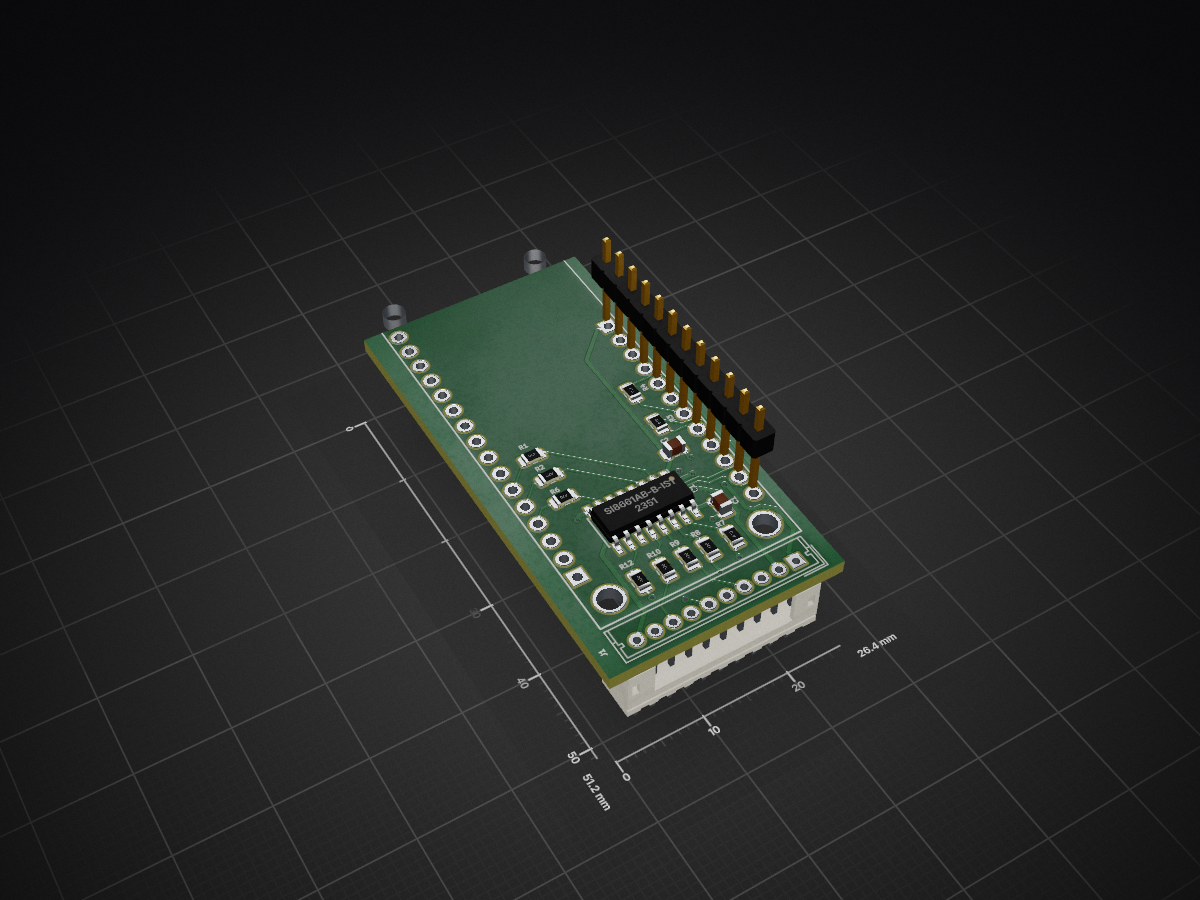
Din isolated SPI is an open-source printed circuit board by BitKnitting, from the BitKnitting/FitHome_Controller_PCB repository on GitHub. It is a 2-layer board of 26.4 × 51.2 mm with 16 parts on 24 nets, routed with 122 tracks and 12 vias.
It is built around the SI8661AB-B-IS1. Its parts include 10 resistors, 2 capacitors, 1 IC and 1 connector. It belongs with the radio and wireless boards of this library.
The goal of this PCB is to supply a Feather to provide the CPU and networking.
The meter and CPU talk to each other using SPI. I just can't map SPI between CPUs and their slaves enough times not to get confused by the differing nomenclatures. Tisham's labeling of SPI used the SI/SO nomenclature on the slave (the meters) and MOSI/MISO on the master (the CPU). This maps to:

I plan to support Feather LoRa and Huzzah. This way, I can do either RFM95 or wifi.
Previously, I used pins 0 and 15 for the two CS pins. Here is the pinout diagram for the Huzzah:

The "0" and "15" refer to how the IDE (Arduino, CP) identify the pin. The "physical pin" for 0 is 12 and for 15 is 10. Because all of this confuses me quickly, I can best find these by noting:
Here is the pinout diagram for the LoRa:

I keep getting different Feathers that need CP installed. Steps to install:
I'm conflicted if the Huzzah if Adafruit has dropped support for the Huzzah. The .bin is included in the latest releases. So I'm using that. You'll need the ampy and esptool tools installed.
$ export PORT=/dev/tty.SLAB_USBtoUART
$ esptool.py -p $PORT erase_flashesptool.py -p /dev/cu.SLAB_USBtoUART write_flash --flash_size=detect 0 cphuzzah.bin| Qty | Value | Footprint | References |
|---|---|---|---|
| 10 | 47 | Resistor_SMD:R_0805_2012Metric | R1, R2, R3, R4, R6, R7, R8, R9, R10, R12 |
| 2 | .1u | Capacitor_SMD:C_0805_2012Metric | C1, C2 |
| 1 | ADAFRUIT_FEATHERWING_FitHome | HappyDayEnergyMonitor:ADAFRUIT_FEATHER | MS1 |
| 1 | CONN_01X10 | Connectors_Molex:Molex_MicroLatch-53253-1070_10x2.00mm_Straight | J1 |
| 1 | LOGO | Whatnick_logo:Whatnick_logo | G1 |
| 1 | SI8661AB-B-IS1 | Housings_SOIC:SOIC-16_3.9x9.9mm_Pitch1.27mm | U1 |
google/mozc-devices
Circuit diagrams and firmware source code for Gboard DIY keyboards

conorpp/u2f-zero
U2F USB token optimized for physical security, affordability, and style

rusefi/rusefi
rusefi - GPL internal combustion engine control unit

VoronDesign/Voron-Hardware
Cool Hardware designed by the Voron Design group

hoglet67/RGBtoHDMI
Bare-metal Raspberry Pi project that provides pixel-perfect sampling of Retro Computer RGB/YUV video and conversion to HDMI

hackclub/OnBoard
💡 Join 1,000 teenagers and make your first PCB with a $100 grant!


It measures 26.4 × 51.2 mm and has 2 copper layers, 1.6 mm thick.
16 parts, built around the SI8661AB-B-IS1. The full list of its parts is on this page, with links to each part's symbol and footprint where PCBKit's library has them.
From the BitKnitting/FitHome_Controller_PCB repository on GitHub, at the commit this page was made from: the board is din_isolated_SPI.kicad_pcb. PCBKit opens the board in the browser, with nothing to install.
Its repository states no licence, so its author keeps all rights: ask BitKnitting before reusing the design.