4 layers90 × 70 mm
InclinationMeter
soldernerd/InclinationMeter
A battery-powered, Bluetooth-enabled precision electronic level instrument for machine tool geometry inspection and granite surface plate qualification.
118 parts

 BenjaminK100/MacroPad
Custum diy macropad for hackclub/ my desk setup
Hackpad is an open-source printed circuit board by BenjaminK100, from the BenjaminK100/MacroPad repository on GitHub. It is a 2-layer board of 76.2 × 76.8 mm with 31 parts on 45 nets, routed with 180 tracks and 15 vias.
It is built around the 1N4148WT, B12AP and B2B-PH-K-S, with the G12AP and PEC11R-4215F-S0024 among its other parts. Its parts include 14 switches, 12 diodes, 2 ICs and 1 connector. It belongs with the keyboards and input boards and the nRF52 and nRF5x boards of this library.


this is my custom key macropad using a seeed xiao rp2040. i built it mostly because i wanted something actually to help with Spotiy and shortcuts
it’s got a rotary encoder for volume, a small oled screen, and a 3x4 matrix its daily stuff like oping apps shuffle music ect. right its
open firefox, spotify, discord control volume with the knob mute/unmute my mic toggle vpn run a timer that shows how long i’ve been working show status on the screen (mic, vpn, timer) still depding on wat annimation to use
firmware is just circuitpython since it’s easy to change stuff quickly. might switch to qmk later but this works fine for now.
future stuff i might add:
better screen ui (icons instead of text) animations different modes depending on what i’m doing proper linux integration instead of basic shortcuts
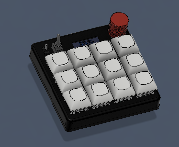


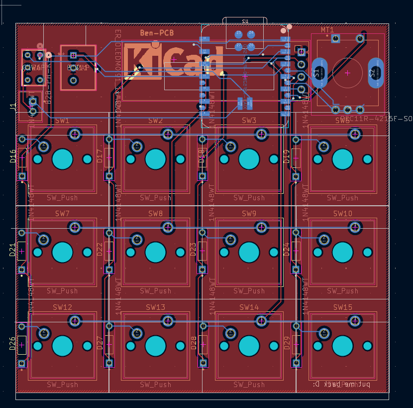
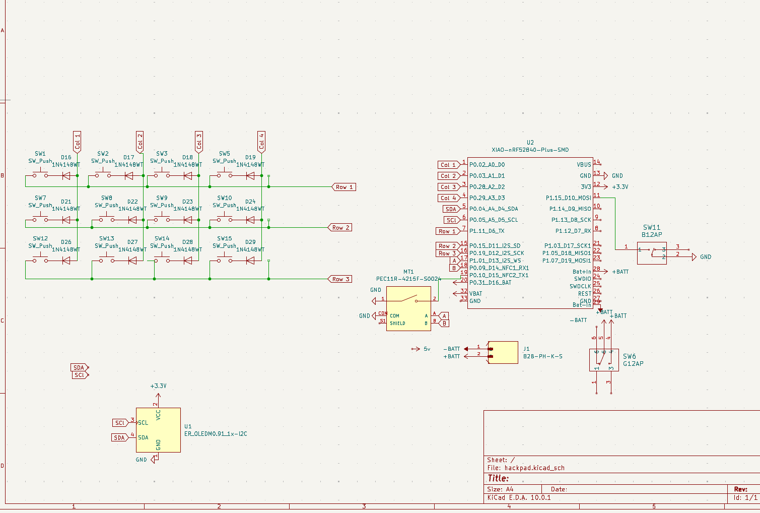
BOM Seeed XIAO RP2040 1N4148 Diodes, 12, MX-Style switches, 12 MX-Style switches,0.91 inch OLED display, keycaps, 4x M3x16mm 4x M3x5mx4mm heatset inserts
| Qty | Value | Footprint | References |
|---|---|---|---|
| 12 | 1N4148WT | 1N4148:DIOAD753W49L380D172B | D16, D17, D18, D19, D21, D22, D23, D24, D26, D27, D28, D29 |
| 12 | SW_Push | Button_Switch_Keyboard:SW_Cherry_MX_1.00u_PCB | SW1, SW2, SW3, SW5, SW7, SW8, SW9, SW10, SW12, SW13, SW14, SW15 |
| 1 | B12AP | footprints:B12AP_NKK | SW11 |
| 1 | B2B-PH-K-S | B2B_PH_K_S:JST_B2B-PH-K-S | J1 |
| 1 | ER_OLEDM0.91_1x-I2C | Display:ER_OLEDM0.91_1x-I2C | U1 |
| 1 | G12AP | ul_G12AP:G12AP_NKK | SW6 |
| 1 | PEC11R-4215F-S0024 | PEC11R-4215F-S0024:XDCR_PEC11R-4215F-S0024 | MT1 |
| 1 | XIAO-nRF52840-Plus-SMD | New_XIAO_Series_Footprints:XIAO-nRF52840-Plus-SMD | U2 |
The 30 most common of 31 parts.
It measures 76.2 × 76.8 mm and has 2 copper layers, 1.6 mm thick.
31 parts, built around the 1N4148WT, B12AP, B2B-PH-K-S and G12AP. The full list of its parts is on this page, with links to each part's symbol and footprint where PCBKit's library has them.
From the BenjaminK100/MacroPad repository on GitHub, at the commit this page was made from: the board is PCB/hackpad.kicad_pcb and its schematic PCB/hackpad.kicad_sch. PCBKit opens the board in the browser, with nothing to install.
Its repository states no licence, so its author keeps all rights: ask BenjaminK100 before reusing the design.
soldernerd/InclinationMeter
A battery-powered, Bluetooth-enabled precision electronic level instrument for machine tool geometry inspection and granite surface plate qualification.

wattnotions/povbot2
Look in 3dprint folder to find a 3mf file with the chassis , camera holder and wheels ready to print.

Xenii1642/USB-GC2
Meet the new generation of USB-C GameCube Power Board. Now compatible with both 12V and 15V chargers. Two voltages, twice the potential.

FeruzTopalov/spoke
Standalone LoRa-based real-time off-grid relative GPS navigation for group of up to 5 people. Improved version of LRNS Eleph

greigs/OpenBrickGB
Functional / Playable Lego Game Boy Electronics - PCB Design Files

Andresse2020/NovaDrone-Hardware
Complete electronic system design for a high-performance quadcopter drone, developed entirely from scratch. Includes power distribution, motor control, flight stabilization, sensor integration, and communication…


kennyegan/Snowboard-Wearable
This system is designed to help snowboarders visualize, analyze, and improve their performance using a wearable IoT device and a companion mobile application.