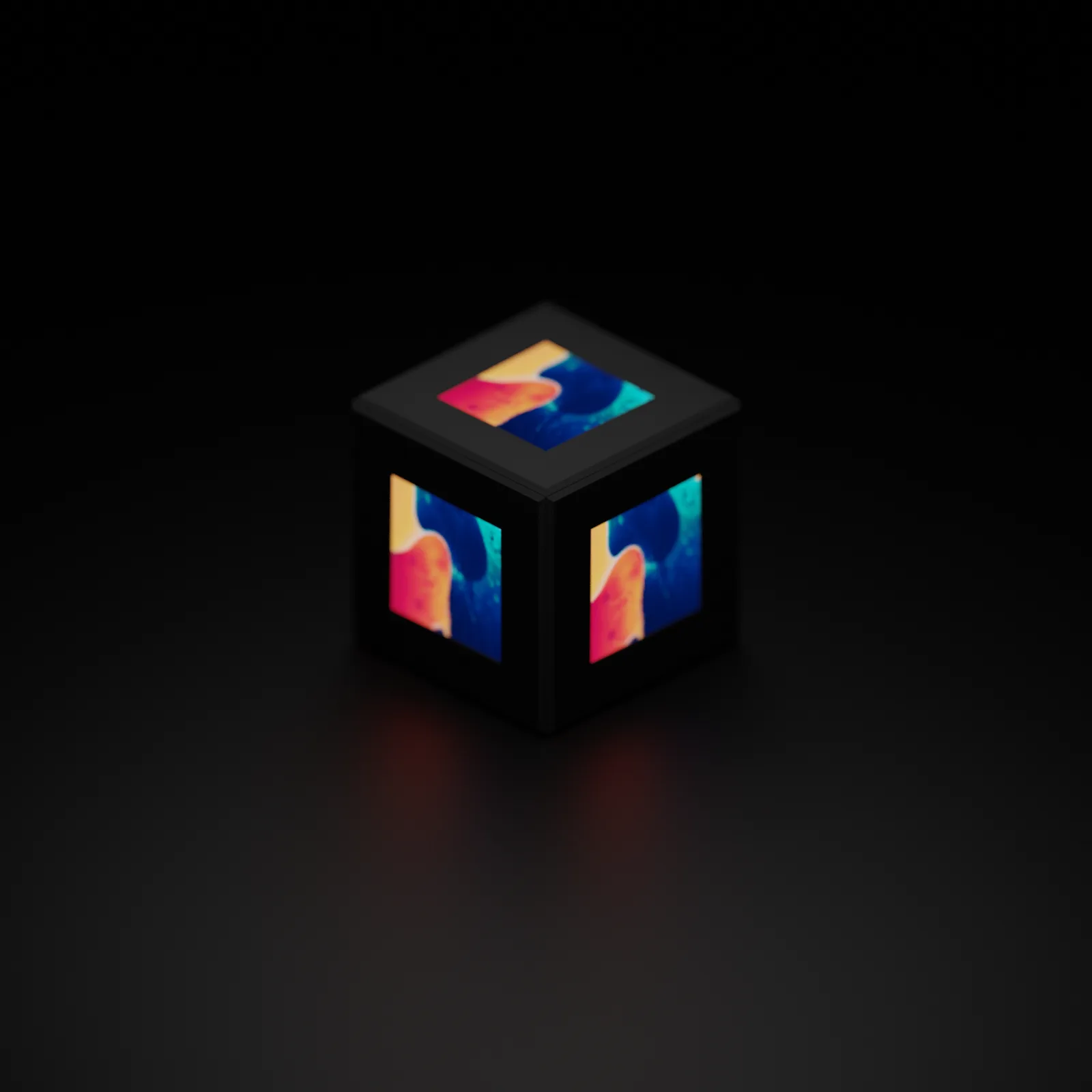
CUBE is a miniature, six-faced OLED display cube built from a stack of custom interconnected PCBs. The current design combines an ESP32-S2 motherboard, five further display boards, a magnet-held 3D-printed frame and…
CUBE is an open-source printed circuit board by BenjaminJAnderson, from the BenjaminJAnderson/CUBE repository on GitHub, published under the MIT licence. It is a 2-layer board of 38 × 37.9 mm with 12 parts on 34 nets, routed with 152 tracks and 91 vias.
It is built around the 4DOLED-282815. Its parts include 5 capacitors, 2 resistors, 2 diodes, 2 connectors and 1 IC.
CUBE is a miniature, six-faced OLED display cube built from a stack of custom interconnected PCBs. The current design combines an ESP32-S2 motherboard, five further display boards, a magnet-held 3D-printed frame and bring-up firmware for SPI displays and motion sensing.
Overview
CUBE is a handheld, self-contained display object rather than a conventional LED matrix. Each of its six faces carries a 1.5-inch, 128×128 RGB OLED module driven by an SSD1351 controller, giving 98,304 addressable pixels across the cube. The aim is to make a small object whose faces can show independent graphics and respond to movement, while remaining easy to open, charge and repair.
The project began in December 2021 after seeing Greg Davill's miniature LED cube and Pol Pla's research on Display Blocks. Both demonstrated the appeal of a compact, tactile display device. CUBE takes that idea in a different direction: instead of an FPGA and an LED matrix, it uses a microcontroller, six square OLED modules and a modular PCB-and-frame construction.
Status: design-stage prototype. The repository records work from December 2021 to May 2022. It contains the electrical and mechanical design files, photographs of a fabricated motherboard and several printed frame prototypes, and display and IMU bring-up sketches. The final assembled cube and an integrated application firmware are not present.
Features
Six active faces: one 128×128 RGB OLED on the motherboard and one on each of the five display boards.
Shared SPI display bus: all six SSD1351 displays share clock, data and data/command lines, with a separate chip-select line for each face.
Daisy-chained construction: 20-way, 0.5 mm pitch flat flexible cables carry power and SPI between boards, allowing the cube to be unfolded for assembly and servicing.
ESP32-S2 motherboard: native USB, external-antenna module footprint, ICM-20602 six-axis IMU, USB-C input, LiPo charger with load sharing, 3.3 V regulation and a 13 V boost converter for the OLEDs.
Modular display boards: D2–D6 each carry one display, two FFC connectors and the necessary decoupling and termination. The repeated design allows a single side to be revised independently later.
Magnet-held frame: FreeCAD models and STEP/STL exports for the enclosure, using 3 mm neodymium magnets to join printed panels.
Bring-up software: Arduino sketches that test one display at a time up to six displays, exercise the Adafruit GFX drawing primitives, and demonstrate IMU orientation output.
Technologies
KiCad: schematic capture, PCB layout and fabrication outputs. D1 uses the KiCad 6 project format; D2–D6 use the earlier .sch and .pro format.
ESP32-S2: the ESP32-S2-MINI-1U supplies the processing, Wi-Fi, native USB and external-antenna option.
SSD1351 and Adafruit GFX: display driver and graphics library used by the OLED modules and test sketches.
C/C++ with the Arduino framework: firmware bring-up sketches for the displays and IMU.
FreeCAD: mechanical design of the frame, including the panel and magnet layouts.
Blender: rendered presentation of the assembled cube.
JLCPCB: SLA 3D printing service used for the individual frame panels.
Gallery
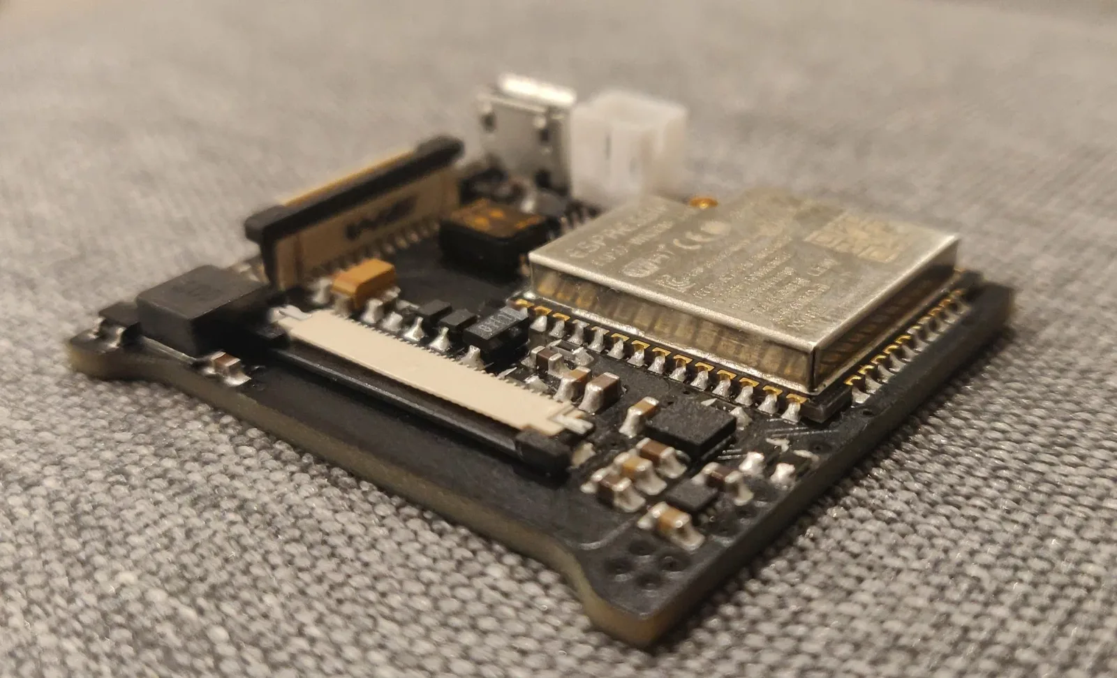
The assembled motherboard, showing the ESP32-S2 module, USB-C connector, battery connector, FFC connector and power circuitry.
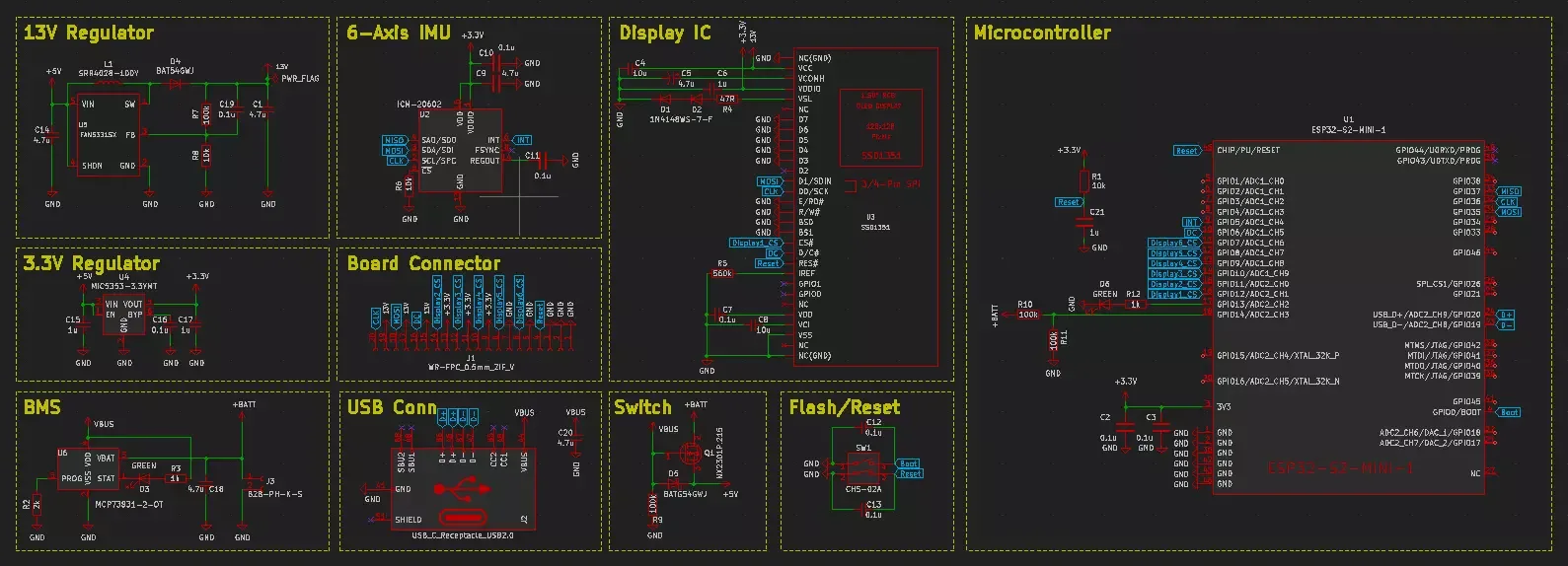
Motherboard schematic sheets covering the 13 V and 3.3 V supplies, battery management, USB input, IMU, display interface and ESP32-S2.
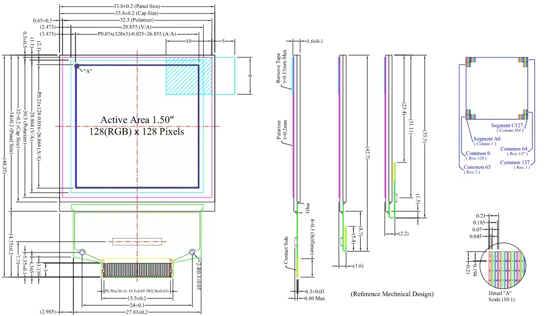
Mechanical reference for the 1.5-inch, 128×128 RGB OLED module, including its active area, bezel and FFC tail.
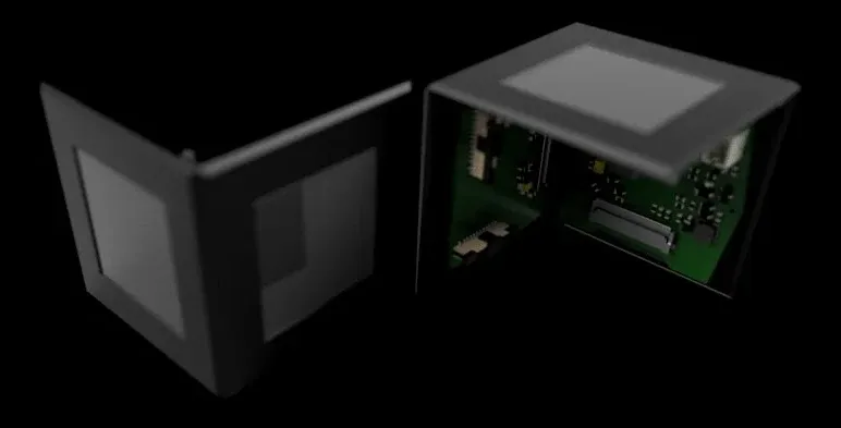
Two frame halves with the PCB assembly test-fitted inside.
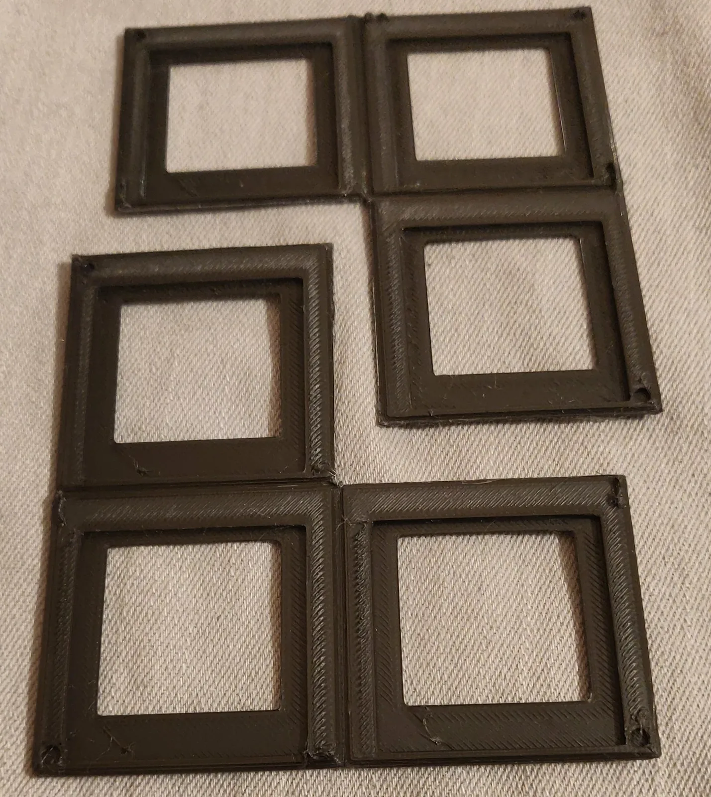
An early FDM-printed frame, printed flat and folded like origami to avoid overhangs.
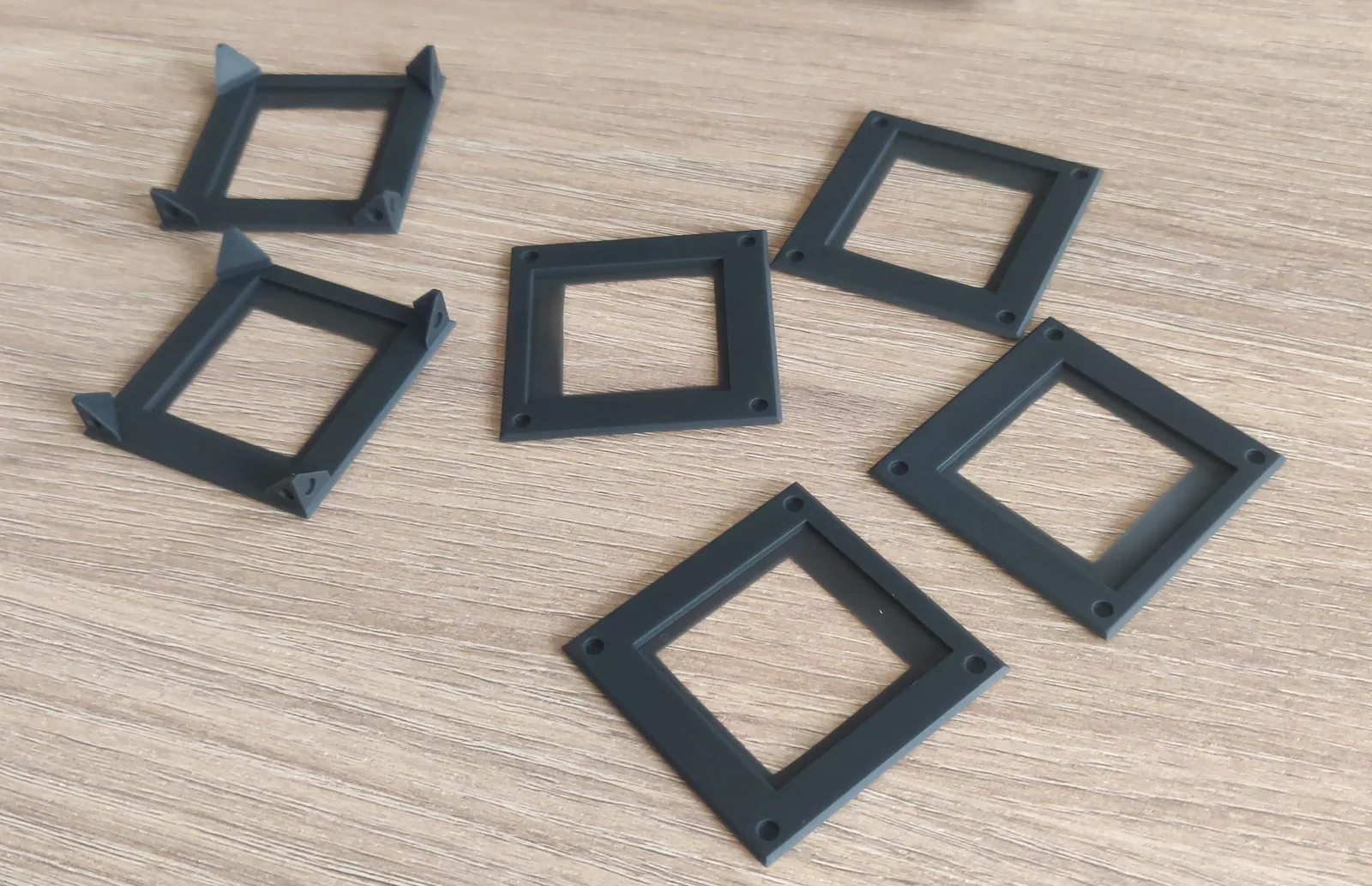
Individual SLA-printed panels with magnet pockets, produced through JLCPCB's 3D printing service.
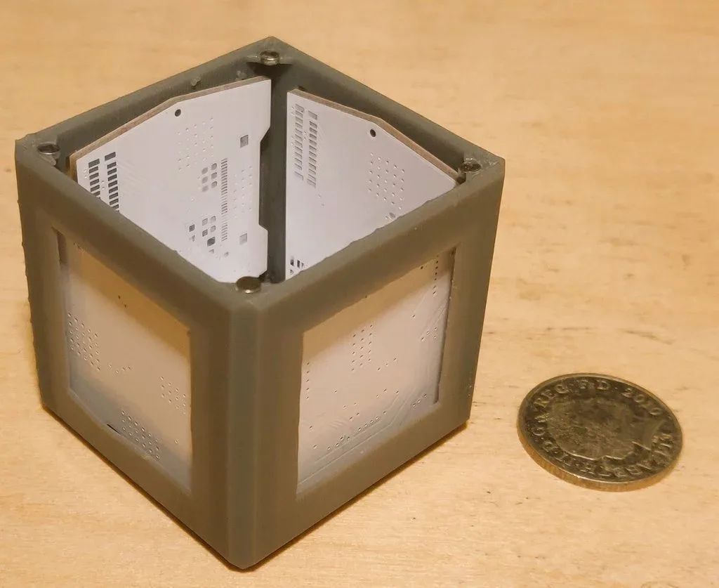
A PCB and display test-fitted into a printed frame panel.
Technical Details
System architecture
CUBE is built from six boards arranged as the faces of a cube. D1 is the motherboard and also carries one display. D2–D6 are display boards with the same electrical function: each accepts the incoming bus, drives one OLED and passes the bus to the next face. The boards are approximately 38 mm across and use two copper layers. The FreeCAD frame envelope is approximately 52 mm cubed.
The interconnect is a 20-way, 0.5 mm pitch FFC bus. It carries the shared SPI clock and data lines, the data/command line, 3.3 V, the 13 V OLED supply, ground and the chip-select lines that have not yet been consumed. D1 uses one select locally and forwards five to D2. Each subsequent board consumes one select and forwards the remainder, so the number of active select lines decreases along the chain until, in the intended design, D6 receives the final line. Because every display has its own chip-select, the microcontroller can update one face without disturbing the others.
Motherboard
The motherboard is built around an ESP32-S2-MINI-1U. The module's native USB interface removes the need for a separate USB-to-UART bridge, reducing component count and board area. The 1U variant was selected for its external-antenna option.
The main subsystems are:
Power input and battery management: a USB-C receptacle feeds a MCP73831 LiPo charger. A P-channel MOSFET and Schottky diode provide load sharing between USB and battery power. A 2-pin JST PH connector accepts the battery.
Regulation: a MIC5353 provides the 3.3 V rail, while a FAN5331 boost converter generates the 13 V bias required by the OLED modules.
Sensing: an ICM-20602 accelerometer and gyroscope share the SPI bus and provide an interrupt output.
Display interface: a 20-pin FFC connector distributes the bus to the first display board. The motherboard also carries one SSD1351 display module on its top face.
Control and status: a two-way DIP switch provides boot and reset control, and green LEDs indicate power and charger status.
Display boards
D2–D6 share the same basic layout and component set, although the chip-select wiring changes along the chain. Each board contains one 1.5-inch 128×128 SSD1351 OLED module, two 20-pin FFC connectors for the daisy chain, decoupling capacitors and series components for the display signals. There is no local microcontroller; all rendering is performed by the ESP32-S2 and sent over the shared bus.
The D6 directory currently contains copies of the D5 files, including the D5 chip-select assignment. This is a known naming and versioning artefact: D6 is intended to be the sixth display face, and the duplicate was left in place so that a single side could be modified later without changing the other four. Before D6 can act as the sixth face, its netlist needs to be changed to consume only Display6_CS.
Mechanical design
The enclosure was developed in FreeCAD and exported as STEP and STL files. The frame is approximately 52 mm cubed and uses 3 mm neodymium magnets to hold its sections together so that the cube can be opened for charging or repair. The repository includes the FreeCAD source, the six wall panels, a compound assembly and several earlier design iterations in Hardware/Frame/OLD.
Three fabrication approaches were explored:
FDM-printed folded frame: the panels were printed flat in ABS and folded like origami. This avoided overhangs and produced a smooth outer surface, but the print quality and tolerances were not good enough for a finished object.
Single-piece SLA lid: an SLA print gave a better surface finish, but the material was brittle and chipped during support removal. Placing PCBs into a frame with five connected panels was also difficult.
Individual magnet panels: each panel was printed separately through JLCPCB's SLA service, allowing the PCBs and displays to be fitted easily. The finish was the best of the three, but the resulting frame was fragile when pressure was applied to opposite corners, and gluing the many magnets was slow and error-prone.
The design direction recorded in the project notes is a final frame made from two evenly sized three-sided sections, printed in SLA, with improved magnet pockets. Keeping each section to three sides makes assembly easier while still allowing the cube to be opened.
Firmware and bring-up
The software is a collection of Arduino sketches rather than a finished application. The sequence in Software/Display/Testing progresses from a single display to test routines for all six faces. 1_Display_SW initialises one display, and the later sketches add calls for more faces. The progression is not fully consistent: 3_Display_SW initialises OLED4 but not OLED3, while 5_Display_SW and 6_Display_SW call drawing routines on the fifth and sixth displays without calling begin() on those objects. The sketches use software SPI with the following pins:
Signal
GPIO
SCLK
36
MOSI
35
DC
5
CS 1
6
CS 2
12
CS 3
14
CS 4
18
CS 5
17
CS 6
11
The display sketches use the Adafruit GFX drawing API and the Adafruit SSD1351 driver. The vendored driver files in Software/Display/lib have been renamed to Multi_SSD1351, but the source still includes Adafruit_SSD1351.h; the upstream Adafruit SSD1351 library should therefore be installed when building the sketches.
The IMU sketches in Software/IMU use an MPU6050 and Jeff Rowberg's DMP library over I2C. They print yaw, pitch and roll over serial for orientation experiments, but they do not drive the ICM-20602 fitted to the motherboard. An ICM-20602 SPI driver and the integration between sensing, rendering and power management remain to be written.
Challenges and Solutions
Driving six displays from one bus
Six displays could not each have a dedicated SPI peripheral, and duplicating the bus would have added wiring and pins. The chosen approach shares clock, data and data/command lines while giving every display its own chip-select. Each board consumes one select line and passes the unused lines to the next board, so the ESP32-S2 can still address any face individually without carrying all six selects to the end of the chain. The staged one-to-six test sketches provide an incremental validation path for this arrangement.
Sourcing a suitable square display
Small, high-resolution square OLED modules are uncommon. The available 1.5-inch 128×128 SSD1351 modules have relatively large bezels, which limits the visible area of each face. The design accepts this trade-off because the modules are readily available, have an integrated controller and use a simple SPI interface. Smaller square OLEDs may become easier to source as the VR and wearable markets grow.
Producing a repeatable frame
Each frame process exposed a different limitation: FDM printing gave poor surface finish and tolerances, SLA printing was brittle and difficult to clean up, and individual magnet panels were fragile under diagonal loads. The current design direction is two three-sided SLA sections with improved magnet pockets, balancing print quality, ease of assembly and serviceability. The prototype frames in the repository are development iterations, not the final enclosure.
Reducing component count
An early constraint was fitting the electronics into a small cube. The ESP32-S2's native USB removed the USB-to-UART bridge and its associated circuitry, and the ESP32-S2-MINI-1U provided the processing and wireless capability in a small module. The remaining power path was kept modular: USB-C input, a LiPo charger with load sharing, a 3.3 V rail and a dedicated 13 V boost for the displays.
Results and Validation
The repository contains evidence of the following work:
A fabricated D1 motherboard, photographed and shown test-fitted in a frame assembly.
KiCad schematics and PCB layouts for the motherboard and display boards.
Printed frame prototypes, including folded FDM frames, SLA panels and a PCB test fit.
Staged display sketches that progress from one display to calls for six faces and exercise drawing primitives.
An IMU orientation sketch using the MPU6050 DMP library.
There is no automated test suite, no captured frame-rate or power-consumption measurements, and no integrated application firmware in this repository. The final cube has not been assembled from the final frame design.
Known limitations:
D6 duplicates the D5 hardware files, including the D5 chip-select wiring, and is not independently versioned.
Several sketches omit begin() calls: 3_Display_SW does not initialise OLED3, and 5_Display_SW and 6_Display_SW do not initialise the fifth and sixth display objects.
The vendored SSD1351 driver is renamed but retains the upstream include name.
The IMU sketch targets the MPU6050, while the motherboard uses the ICM-20602.
The final two-part SLA frame and the integrated firmware are still outstanding.
Getting Started
Prerequisites
KiCad 6 or newer to open the D1 project; the D2–D6 boards use the older KiCad .sch and .pro formats.
FreeCAD to edit the enclosure source and export STEP or STL files.
Arduino IDE or an equivalent Arduino toolchain with the ESP32 board support package for the firmware sketches.
Adafruit GFX and Adafruit SSD1351 libraries for the display sketches.
Jeff Rowberg's MPU6050 library for the IMU demonstration.
Blender if you want to open the presentation render.
For a physical build: six 1.5-inch 128×128 SSD1351 OLED modules, 20-way 0.5 mm FFC cables and connectors, a compatible LiPo battery, 3 mm neodymium magnets and the printed frame parts.
Opening the hardware design
Open Hardware/PCB/D1(Motherboard)/D1(Motherboard).kicad_pro in KiCad for the motherboard. The display boards are in Hardware/PCB/D2 through Hardware/PCB/D6; D6 contains a copy of the D5 project.
The schematic and layout can also be viewed online through CADLAB.io.
Running the firmware
Install the ESP32 board support package and the Adafruit GFX and Adafruit SSD1351 libraries in the Arduino IDE.
Open the desired sketch under Software/Display/Testing. Start with 1_Display_SW for a single display, then move up to 6_Display_SW.
Select the ESP32-S2 board that matches the module on the motherboard.
Check the pin definitions at the top of the sketch against the board revision before uploading. The pin assignments above reflect the test sketches, not a separate board definition.
Add any missing begin() calls (for example, OLED3 in 3_Display_SW, and OLED5 and OLED6 in the later sketches).
Open the Serial Monitor to see the display initialisation and test output.
For the IMU experiment, open Software/IMU/DMP_CodeESP32/DMP_CodeESP32.ino, install the MPU6050 library and connect an MPU6050 over I2C. This sketch is an experiment for the MPU6050 and is not a driver for the ICM-20602 on the motherboard.
Frame and renders
The editable frame source is Hardware/Frame/Frame.FCStd. Exports include Frame-Walls.step, Frame-Left.step, Frame-Compound002.step and Frame-Walls.stl. Earlier frame versions are kept in Hardware/Frame/OLD.
The Blender presentation file is Renders/Blender/Cube Render.blend.
Finalise the enclosure as two three-sided SLA-printed sections with improved magnet pockets.
Assemble a complete six-face cube from the final frame and boards.
Write and document integrated application firmware for rendering, motion sensing and power management.
Add an ICM-20602 SPI driver and connect it to the display application.
Allow individual display-board revisions for each face; D6 remains a duplicate for now.
Credits and Licensing
The project source and design files are released under the MIT License, copyright 2022 Benjamin J Anderson.
Third-party material:
The display driver and graphics code derive from Adafruit's SSD1351 and GFX libraries, which are distributed under the BSD licence. The original SSD1351 library and its licence are included in Software/Display/Resources/Adafruit-SSD1351-library-1.1.0.
The IMU sketches depend on Jeff Rowberg's I2Cdevlib MPU6050 library, which is not bundled in this repository.
Reference sketches in Software/Display/Resources include material from the Rotatey_Balls project, distributed under the MIT licence.
Component datasheets, antenna documentation and vendor reference designs in Hardware/PCB/D1(Motherboard)/Resources remain subject to their publishers' terms.
Design inspiration: Greg Davill's miniature LED cube and Pol Pla's Display Blocks research, linked in the Overview.
It measures 38 × 37.9 mm and has 2 copper layers, 1.6 mm thick.
What parts does the CUBE use?
12 parts, built around the 4DOLED-282815. The full list of its parts is on this page, with links to each part's symbol and footprint where PCBKit's library has them.
Where can I download the CUBE KiCad files?
From the BenjaminJAnderson/CUBE repository on GitHub, at the commit this page was made from: the board is Hardware/PCB/D5/D5.kicad_pcb and its schematic Hardware/PCB/D1(Motherboard)/D1(Motherboard).kicad_sch. PCBKit opens the board in the browser, with nothing to install.
Can I use the CUBE design in my own project?
Its repository publishes it under the MIT licence: you may reuse it on that licence's terms (keep the author's notice, and for a copyleft licence share your changes alike).
CUBE is a miniature, six-faced OLED display cube built from a stack of custom interconnected PCBs. The current design combines an ESP32-S2 motherboard, five further display boards, a magnet-held 3D-printed frame and…
Tap is a nozzle-based z-probe for the V2 and Trident printer designs. The entire toolhead moves to trigger an optical switch. Tap offers many advantages: