
2 layers172.1 × 143.5 mm
AcCCS
IdahoLabResearch/AcCCS
A collection of tools and scripts used to communicate and emulate Electric Vehicle Communication Controllers (EVCC) and Supply Equipment Communication Controllers (SECC).
111 parts19MIT

 bburan/ir-sensor-strobe
A small four‑channel infrared emitter/detector board. Four IR LEDs (OP140) are driven as a single strobed array; four phototransistors (OP550) act as independent detectors, each presenting an analog output to a…
Ir sensor strobe is an open-source printed circuit board by bburan, from the bburan/ir-sensor-strobe repository on GitHub. It is a 2-layer board of 37.5 × 43.5 mm with 27 parts on 18 nets, routed with 66 tracks and 0 vias.
It is built around the TLC555CP. Its parts include 12 resistors, 8 connectors, 5 capacitors, 1 IC and 1 transistor. It belongs with the sensors and measurement boards of this library.
A small four‑channel infrared emitter/detector board. Four IR LEDs (OP140) are driven as a single strobed array; four phototransistors (OP550) act as independent detectors, each presenting an analog output to a downstream acquisition system.
The strobe carrier can come from either an on‑board ~500 Hz oscillator or an external control signal, selected by a jumper at J1. The optoelectronics mount remotely and connect through headers. The board is all through‑hole and is intended to be hand‑soldered.
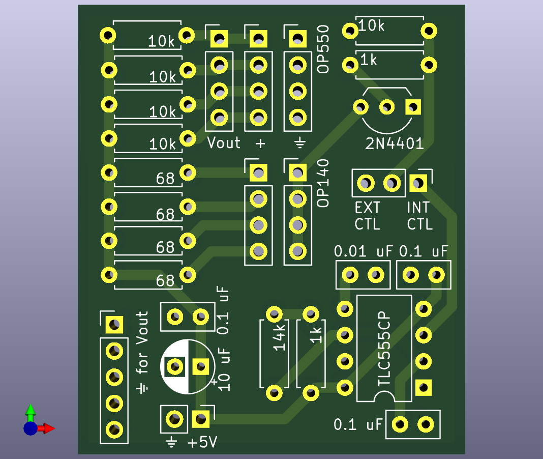
The board contains three functional blocks that share a common +5 V / GND rail.
 +5V ──┬─[68Ω R2]─▷|─ D1 ─┐
       ├─[68Ω R3]─▷|─ D2 ─┤
       ├─[68Ω R4]─▷|─ D3 ─┤   common cathode
       └─[68Ω R5]─▷|─ D4 ─┴────────────┐
                                        │ (collector)
   CTL ──┬─[1kΩ R1]── B  Q1 (2N4401)    ◄
         │                E ── GND
       [10kΩ R10]
         │
        GND
All four IR emitters (D1–D4, OP140) sit between the +5 V rail and a common node, each with its own 68 Ω series resistor (R2–R5) setting the forward current to roughly
I_LED ≈ (5 V − V_f − V_CE(sat)) / 68 Ω ≈ (5 − 1.5 − 0.2) / 68 ≈ 48 mA per LEDThe common cathode node is pulled to ground by low‑side NPN switch Q1, driven from the CTL node through the 1 kΩ base resistor R1 (I_B ≈ 4.1 mA at 5 V). When CTL is high, Q1 saturates and all four LEDs illuminate together; when CTL is low the array is dark. Peak collector current in Q1 is the sum of the four branches, ≈ 190 mA.
R1 is deliberately left at 1 kΩ rather than a lower value. It has to be drivable both by U1 and by an external source (see §1.2); dropping it to 470 Ω would gain only ~5 % LED current while approaching the TLC555's ±10 mA output rating and putting the external drive out of reach of a typical line‑level output.
The 10 kΩ resistor R10 pulls CTL to ground so the array stays dark whenever CTL is undriven or the J1 shunt is removed.
⚠ Q1 orientation differs between board revisions. The current schematic uses an EBC pin mapping (pin 1 = emitter, pin 2 = base, pin 3 = collector), matching a standard TO‑92 2N4401 installed per the silkscreen.
Boards fabricated from the earlier netlist have pads 1 and 3 transposed, and need Q1 inserted rotated 180° (flat face opposite the silkscreen). Built the other way round, Q1 runs reverse‑active (β_R ≈ 5–20 instead of ≈ 150) and the emitters run several times dim with nothing obviously wrong. See §6 for the one‑meter check that tells the two cases apart.
                 +5V
                  │
                [1k R11]
                  │
    ┌─────────────┴── DIS (7)
    │                            ┌──────┐          J1
  [14k R12]      U1  TLC555 ─────┤ Q (3)├──── 1  ○ INT CTL
    │                            └──────┘         │
    ├─────────────┬── THR (6)                   2  ○ ── CTL ── R1 → Q1 base
    │             └── TR  (2)                      │
 [0.1µ C3]                                       3  ○ EXT CTL ── external drive
    │
   GND
U1 is a TLC555 wired as a standard astable:
f = 1.44 / ((R11 + 2·R12) · C3) = 1.44 / ((1k + 28k) · 0.1 µF) ≈ 497 Hz
D = (R11 + R12) / (R11 + 2·R12) = 15k / 29k ≈ 51.7 %
C4 (0.01 µF) decouples the control‑voltage pin; C5 (0.1 µF) is local supply bypass. RESET (pin 4) is tied to +5 V.
J1 selects the strobe source — the silkscreen marks the two ends INT CTL and EXT CTL:
| Shunt | Source | Use |
|---|---|---|
| 1–2 | On‑board oscillator (U1) | Board self‑strobes at ~497 Hz. No host output needed. |
| 2–3 | External drive | Host supplies the carrier on pin 3. |
With no shunt fitted, R10 holds CTL low and the array stays dark.
A CMOS TLC555 is specified rather than a bipolar NE555 deliberately: its output swings close to the rails (a bipolar 555 drops ~1.7 V, starving Q1's base) and it does not inject the large supply transients an NE555 does on each edge, which matters on a board carrying 10 kΩ‑impedance analog sensor lines.
Why ~50 % duty. For a square carrier of fixed peak current, the amplitude recovered at the fundamental is (2·I_pk/π)·sin(πD), maximised at D = 0.5. The maximum is flat, so the astable's 51.7 % costs about 0.15 % — the diode trick often used to force exactly 50 % is unnecessary here.
 +5V ──[10kΩ]──┬──────► Vout (to J2 / J6)
               │ C
              (Q_photo, OP550)
               │ E
              GND (J5)
Each phototransistor (Q2–Q5, OP550) is wired common‑emitter: collector pulled to +5 V through a 10 kΩ load resistor (R6–R9), emitter to ground. The output is taken at the collector:
The response is therefore inverting. The four channels are electrically independent; only the emitter array is strobed, in common.
The detectors are not modulated — only the emitters are. Recovering the signal at the carrier frequency (e.g. quadrature demodulation at ~497 Hz) rejects ambient light, mains‑derived flicker, and the DC offset of each phototransistor, which is what makes the board usable through an AC‑coupled input.
Quantities are per board. All parts are through‑hole. 27 placements, 75 joints.
| Ref(s) | Qty | Value / Part | Package / Footprint | Notes |
|---|---|---|---|---|
| R1, R11 | 2 | 1 kΩ | Axial ¼ W, 7.62 mm pitch (DIN0207) | Q1 base resistor; 555 charge resistor |
| R2, R3, R4, R5 | 4 | 68 Ω | Axial ¼ W, 7.62 mm pitch | LED ballast, ~48 mA each (82 mW worst case) |
| R6, R7, R8, R9 | 4 | 10 kΩ | Axial ¼ W, 7.62 mm pitch | Phototransistor collector load |
| R10 | 1 | 10 kΩ | Axial ¼ W, 7.62 mm pitch | CTL pulldown |
| R12 | 1 | 14 kΩ | Axial ¼ W, 7.62 mm pitch | 555 timing (E96 value) |
| C1 | 1 | 10 µF | Radial electrolytic, 2.5 mm pitch (polarized) | Bulk bypass at J4; observe polarity |
| C2, C3, C5 | 3 | 0.1 µF | Ceramic disc, 2.5 mm pitch | C2 supply HF bypass, C3 555 timing, C5 U1 local bypass |
| C4 | 1 | 0.01 µF | Ceramic disc, 2.5 mm pitch | 555 control‑voltage decoupling |
| U1 | 1 | TLC555CP | DIP‑8, 7.62 mm row spacing | CMOS 555 — do not substitute NE555 (see §1.2) |
| Q1 | 1 | 2N4401 | TO‑92 (inline) | EBC pinout. See orientation warning in §1.1 |
| J1 | 1 | 3‑pin header | 2.54 mm PinHeader 1×03 | Strobe source select (INT CTL / EXT CTL) |
| J2 | 1 | 4‑pin header | 2.54 mm PinHeader 1×04 | Detector outputs to acquisition |
| J3 | 1 | 5‑pin header | 2.54 mm PinHeader 1×05 | Ground bus for the Vout harness |
| J4 | 1 | 2‑pin header | 2.54 mm PinHeader 1×02 | Power in: pin 1 = +5 V, pin 2 = GND |
| J5 | 1 | 4‑pin header | 2.54 mm PinHeader 1×04 | OP550 return (emitters, all GND) |
| J6 | 1 | 4‑pin header | 2.54 mm PinHeader 1×04 | OP550 out (collectors) |
| J7 | 1 | 4‑pin header | 2.54 mm PinHeader 1×04 | OP140 in (common cathode return) |
| J8 | 1 | 4‑pin header | 2.54 mm PinHeader 1×04 | OP140 out (anodes) |
Off‑board optoelectronics (not on the PCB, wired via the harness — see §3.2):
| Ref(s) | Qty | Part | Notes |
|---|---|---|---|
| D1, D2, D3, D4 | 4 | OP140 IR emitter | Anode to J8, cathode to J7 |
| Q2, Q3, Q4, Q5 | 4 | OP550 phototransistor | Collector to J6, emitter to J5 |
Emitter/detector wavelength. Confirm the detector's spectral response overlaps the emitter's output for your specific parts before ordering in quantity, and consult current datasheets for lead configuration.
Sourcing note. Through‑hole ICs are being discontinued industry‑wide. If TLC555CP (DIP‑8) becomes hard to source, the SOIC‑8 TLC555CD is cheaper and better stocked, but requires a footprint change.
All through‑hole, hand‑solder friendly. Nothing requires reflow. Budget roughly 20–30 minutes per board.
Populate lowest‑profile parts first so the board sits flat while you work:
+ lead to the +
pad; the silkscreen band indicates the negative side.Clean flux as appropriate and inspect for bridges, especially at the connector rows.
The OP140 emitters and OP550 detectors are not mounted on the PCB. They are wired on flying leads so they can be positioned on a fixture — aimed across a nose‑poke or lick spout, for example. Four headers carry them:
| Header | Silk | Carries | Pin mapping |
|---|---|---|---|
| J8 | OP140 | LED anodes (one per channel, each via its own ballast) | pin 1 → D4, pin 2 → D3, pin 3 → D2, pin 4 → D1 |
| J7 | OP140 | LED cathodes — all four pins common, returning to Q1 | any pin; one per LED keeps the harness symmetric |
| J6 | OP550 | Detector collectors (the outputs) | pin 1 → Q2, pin 2 → Q3, pin 3 → Q4, pin 4 → Q5 |
| J5 | OP550 | Detector emitters — all four pins are GND | one per detector, giving each channel its own return |
⚠ J8's pin order is reversed relative to the D1–D4 reference designators (pin 1 is D4, pin 4 is D1). J6 runs in order (pin 1 = Q2 … pin 4 = Q5). Check this when building the harness; getting it backwards silently swaps which physical emitter pairs with which detector channel.
Polarity out at the remote device still matters: the OP140 anode goes to J8 and its cathode to J7; the OP550 collector goes to J6 and its emitter to J5. A reversed LED will not emit; a reversed phototransistor will not conduct properly.
Giving each detector its own return conductor to J5 rather than daisy‑chaining them keeps inter‑channel ground coupling down on long harnesses.
Generate Gerbers/drill from IR sensor strobe.kicad_pcb (KiCad 8:
File → Fabrication Outputs → Gerbers and Drill Files), or order directly from
the KiCad project at any standard fab.
| Parameter | Value |
|---|---|
| Layers | 2 (F.Cu / B.Cu) |
| Board size | ≈ 37.5 mm × 43.5 mm |
| Thickness | 1.6 mm |
| Material | FR‑4 |
| Finish | HASL or ENIG (either is fine — all THT) |
| Min feature | Default KiCad clearances; no fine‑pitch parts, so any vendor's economy process is adequate |
| Silkscreen | Both sides used (title/attribution on back) |
There are no controlled‑impedance, high‑voltage, or thermal requirements.
The back silkscreen reads "Strobed IR emitter/sensor w/ internal generator", which distinguishes this revision from the earlier board — worth checking before assembly, since Q1's orientation differs between the two (§1.1).
If ordering assembled: the board is 100 % through‑hole, which is the worst‑priced category at every CM because it is hand‑soldered. At low quantity hand assembly is usually cheaper than the setup fees. If assembly cost matters at volume, converting the passives to 0805 and U1 to SOIC‑8 moves the bulk of the work onto automated SMT and leaves only the nine connectors to solder by hand.
| Connector | Pins | Signal | Direction | Description |
|---|---|---|---|---|
| J4 (Power) | 1 | +5 V | in | Board supply. |
| 2 | GND | in | Supply return. | |
| J1 (CTL select) | 1 | INT CTL | — | On‑board oscillator output (U1 pin 3). |
| 2 | CTL | — | Q1 base drive. Shunt 1–2 for internal, 2–3 for external. | |
| 3 | EXT CTL | in | External strobe input. Logic high → all IR LEDs on. | |
| J2 (Vout) | 1–4 | Vout[1..4] | out | The four detector outputs, same nets as J6. High ≈ dark, low ≈ illuminated. |
| J3 (GND) | 1–5 | GND | — | Ground bus; all five pins common. Return/reference for the Vout harness. |
| J5 (OP550 return) | 1–4 | GND | — | Detector emitter returns. |
| J6 (OP550 out) | 1–4 | Vout[1..4] | — | Detector collectors — the remote sensor cable. |
| J7 (OP140 in) | 1–4 | LED common cathode | — | All four pins common, returning to Q1's collector. |
| J8 (OP140 out) | 1–4 | LED anodes | — | One per channel, reverse order — see §3.2. |
J2 and J6 are the same four nets: J6 faces the remote sensor harness, J2 faces the acquisition system. That is deliberate fan‑out, not a duplicate.
Unpowered: verify J4 polarity. A resistance check from +5 V to GND will briefly show C1/C2 charging before settling high — it should not read a hard short. Confirm C1's polarity.
Power, no J1 shunt: apply +5 V. R10 holds CTL low, so the array is dark. Each Vout on J2 should read ≈ +5 V (detectors dark, pulled up through 10 kΩ). Quiescent current is small.
Oscillator: fit the J1 shunt on 1–2 and scope U1 pin 3. Expect a roughly square wave near 497 Hz at ~52 % duty, swinging close to the rails. If it sits stuck at either rail, check RESET (pin 4) is at +5 V and that R12 is the 14 kΩ part, not a stray 10 kΩ.
Emitter current — the Q1 orientation check. With the strobe running, measure the DC voltage across any one 68 Ω ballast (R2–R5):
Confirm IR emission with a phone camera (a faint pale/purple glow on many sensors) or an IR‑sensitive card.
Detector response: with the emitters running, illuminate a detector (reflect off a nearby surface, or point an IR source at it). Its Vout should show the carrier, and the amplitude should collapse when the beam is blocked. Repeat per channel.
End to end: demodulate each channel at the carrier frequency and confirm that breaking the beam produces a large, unambiguous amplitude drop.
| Qty | Value | Footprint | References |
|---|---|---|---|
| 5 | 10k | Resistor_THT:R_Axial_DIN0207_L6.3mm_D2.5mm_P7.62mm_Horizontal | R6, R7, R8, R9, R10 |
| 4 | 68 | Resistor_THT:R_Axial_DIN0207_L6.3mm_D2.5mm_P7.62mm_Horizontal | R2, R3, R4, R5 |
| 3 | 0.1 uF | Capacitor_THT:C_Disc_D5.0mm_W2.5mm_P2.50mm | C2, C3, C5 |
| 2 | 1k | Resistor_THT:R_Axial_DIN0207_L6.3mm_D2.5mm_P7.62mm_Horizontal | R1, R11 |
| 1 | 0.01 uF | Capacitor_THT:C_Disc_D5.0mm_W2.5mm_P2.50mm | C4 |
| 1 | 10 uF | Capacitor_THT:CP_Radial_D5.0mm_P2.50mm | C1 |
| 1 | 14k | Resistor_THT:R_Axial_DIN0207_L6.3mm_D2.5mm_P7.62mm_Horizontal | R12 |
| 1 | 2N4401 | Package_TO_SOT_THT:TO-92_Inline_Wide | Q1 |
| 1 | CTL select | Connector_PinHeader_2.54mm:PinHeader_1x03_P2.54mm_Vertical | J1 |
| 1 | Conn_01x02 | Connector_PinHeader_2.54mm:PinHeader_1x02_P2.54mm_Vertical | J4 |
| 1 | Conn_01x05 | Connector_PinHeader_2.54mm:PinHeader_1x05_P2.54mm_Vertical | J3 |
| 1 | OP140 in | Connector_PinHeader_2.54mm:PinHeader_1x04_P2.54mm_Vertical | J7 |
| 1 | OP140 out | Connector_PinHeader_2.54mm:PinHeader_1x04_P2.54mm_Vertical | J8 |
| 1 | OP550 out | Connector_PinHeader_2.54mm:PinHeader_1x04_P2.54mm_Vertical | J6 |
| 1 | OP550 return | Connector_PinHeader_2.54mm:PinHeader_1x04_P2.54mm_Vertical | J5 |
| 1 | Sensors | Connector_PinHeader_2.54mm:PinHeader_1x04_P2.54mm_Vertical | J2 |
| 1 | TLC555CP | Package_DIP:DIP-8_W7.62mm | U1 |
It measures 37.5 × 43.5 mm and has 2 copper layers, 1.6 mm thick.
27 parts, built around the TLC555CP. The full list of its parts is on this page, with links to each part's symbol and footprint where PCBKit's library has them.
From the bburan/ir-sensor-strobe repository on GitHub, at the commit this page was made from: the board is IR sensor strobe.kicad_pcb and its schematic IR sensor strobe.kicad_sch. PCBKit opens the board in the browser, with nothing to install.
Its repository states no licence, so its author keeps all rights: ask bburan before reusing the design.
IdahoLabResearch/AcCCS
A collection of tools and scripts used to communicate and emulate Electric Vehicle Communication Controllers (EVCC) and Supply Equipment Communication Controllers (SECC).

espena/light-barrier
Garage door light barrier. KiCad project with schematics and PCB layout.

FernandoVB01/Circuito-Disparo-Laser-CO2
Diseño Básico de Circuito para Disparo PCB CO2

GabrielJaejus/EV
This project is the result of our efforts to find COTS hardware and existing open source software capable of communicating via HomePlug GreenPHY (HPGP) with CCS enabled vehicles and charging stations.


alexanderenrique/smart_tbird
Smart Thunderbird vehicle electronics — ESP32 nodes, alternator delay, display, and tooling.

finnandreh/codex-cad-electronics-lab
Sanitized FreeCAD and KiCad source, exports, checks and videos from Finn Andre Hotvedt's Codex-assisted CAD lab.