2 layers21.6 × 31.8 mm

 bareware/pcb-STM32G030Fx
STM32G030F Development Board
Board panel is an open-source printed circuit board by bareware, from the bareware/pcb-STM32G030Fx repository on GitHub, published under the MIT licence. It is a 2-layer board of 92.4 × 79.5 mm with 313 parts on 176 nets, routed with 1,072 tracks and 64 vias.
Its parts include 24 capacitors, 24 connectors, 16 resistors, 16 diodes and 16 switches. It belongs with the STM32 boards of this library.
STM32G030Fx Development Board
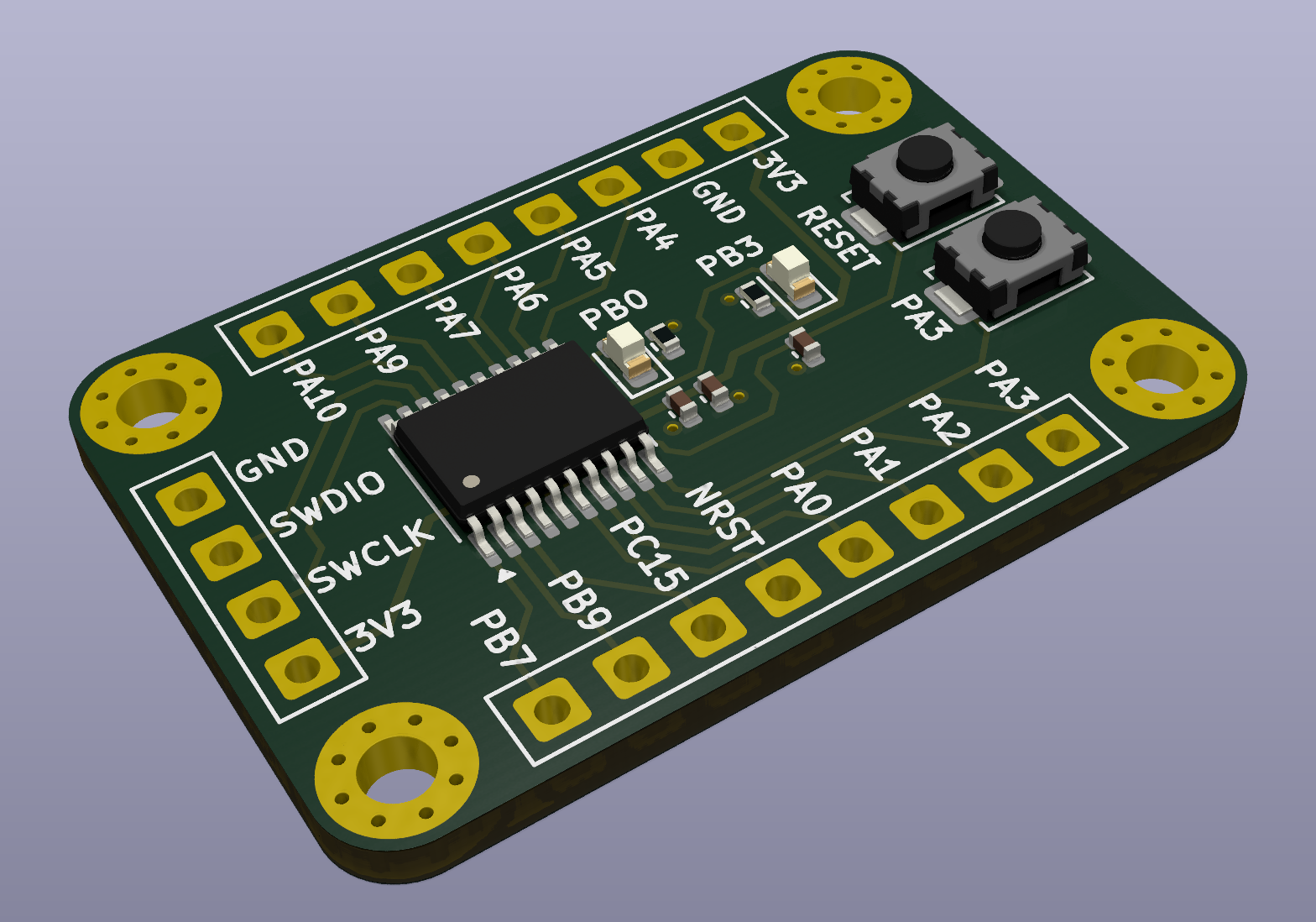
| Qty | Value | Footprint | References |
|---|---|---|---|
| 171 | NPTH | NPTH | KiKit_MB_10_1, KiKit_MB_10_2, KiKit_MB_10_3, KiKit_MB_10_4, KiKit_MB_10_5, KiKit_MB_10_6, KiKit_MB_11_1, KiKit_MB_11_2, KiKit_MB_11_3, KiKit_MB_11_4, KiKit_MB_11_5, KiKit_MB_11_6, KiKit_MB_12_1, KiKit_MB_12_2, KiKit_MB_12_3, KiKit_MB_12_4 +155 |
| 32 | MountingHole | MountingHole:MountingHole_2.2mm_M2_Pad_Via | H1, H1, H1, H1, H1, H1, H1, H1, H2, H2, H2, H2, H2, H2, H2, H2 +16 |
| 16 | 100n | Capacitor_SMD:C_0402_1005Metric | C2, C2, C2, C2, C2, C2, C2, C2, C3, C3, C3, C3, C3, C3, C3, C3 |
| 16 | 1k | Resistor_SMD:R_0402_1005Metric | R1, R1, R1, R1, R1, R1, R1, R1, R2, R2, R2, R2, R2, R2, R2, R2 |
| 16 | Conn_01x08 | Connector_PinHeader_2.54mm:PinHeader_1x08_P2.54mm_Vertical | J2, J2, J2, J2, J2, J2, J2, J2, J3, J3, J3, J3, J3, J3, J3, J3 |
| 16 | ~ | LED_SMD:LED_0603_1608Metric | D1, D1, D1, D1, D1, D1, D1, D1, D2, D2, D2, D2, D2, D2, D2, D2 |
| 16 | ~ | Button_Switch_SMD:SW_SPST_TS-1088-xR020 | SW1, SW1, SW1, SW1, SW1, SW1, SW1, SW1, SW2, SW2, SW2, SW2, SW2, SW2, SW2, SW2 |
| 8 | 4u7 | Capacitor_SMD:C_0402_1005Metric | C1, C1, C1, C1, C1, C1, C1, C1 |
| 8 | DEBUG | Connector_PinHeader_2.54mm:PinHeader_1x04_P2.54mm_Vertical | J1, J1, J1, J1, J1, J1, J1, J1 |
| 8 | STM32G030F6Px | Package_SO:TSSOP-20_4.4x6.5mm_P0.65mm | U1, U1, U1, U1, U1, U1, U1, U1 |
| 6 | Fiducial | Fiducial | KiKit_FID_B_1, KiKit_FID_B_2, KiKit_FID_B_3, KiKit_FID_T_1, KiKit_FID_T_2, KiKit_FID_T_3 |


Mozzie-AU/LeafOBC-WafflePlate
Reverse engineering the "waffle plate" power module from the 2012 Nissan Leaf on-board charger (OBC), with the goal of building a functional replica from regular, off-the-shelf components.

It measures 92.4 × 79.5 mm and has 2 copper layers, 1.6 mm thick.
313 parts. The full list of its parts is on this page, with links to each part's symbol and footprint where PCBKit's library has them.
From the bareware/pcb-STM32G030Fx repository on GitHub, at the commit this page was made from: the board is panel/rev1/board_panel.kicad_pcb and its schematic board/rev1/board.kicad_sch. PCBKit opens the board in the browser, with nothing to install.
Its repository publishes it under the MIT licence: you may reuse it on that licence's terms (keep the author's notice, and for a copyleft licence share your changes alike).