2 layers450 × 160 mm

 barberd/coco9511pak13
This board is a cartridge for the Tandy Radio Shack TRS-80 Color Computer (CoCo), an 8 bit computer produced between 1980 and 1991. It provides an Arithmetic Processor Unit (APU), the AMD 9511, to the CoCo.
Coco9511pak is an open-source printed circuit board by barberd, from the barberd/coco9511pak repository on GitHub, published under the GPL-3.0 licence. It is a 2-layer board of 98.3 × 107.1 mm with 44 parts on 100 nets, routed with 1,413 tracks and 29 vias.
It is built around the LT1373CN8#PBF, 74LS00SC and 74LS04PC, with the 74LS05P-E, 74LS123FP-E and 74LS30PC among its other parts. Its parts include 17 capacitors, 14 ICs, 7 resistors, 1 diode and 1 switch.


This board is a cartridge for the Tandy Radio Shack TRS-80 Color Computer (CoCo), an 8 bit computer produced between 1980 and 1991. It provides an Arithmetic Processor Unit (APU), the AMD 9511, to the CoCo.
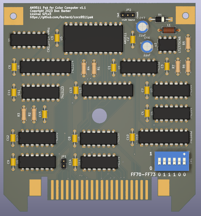
Note the specific component value for X1 on the board's markings and the bill of materials is for the Am9511-4DC; see below if one has a different chip.
Schematic is available here.
A software patch for the Color Computer 3's BASIC can be found in the Basic Patch directory.
Download kicad/coco9511pak-fabrication.zip, then upload it to one's PCB manufacturer when asked to provide Gerber files. Usually this is found under a 'Quote' option on the website. Search "pcb manufacturing" on any major search engine to get several manufacturers. NextPCB and PCBWay are two well-known ones.
Some may have ordered boards and have extra available. Reach out to don @ dgb3.net to explore this.
Use the Bill of Materials to source the components from electronic supply houses such as Mouser, Jameco, or Digi-Key.
Design maintained at https://github.com/barberd/coco9511pak. Kicad and Freerouting were used to design the board.
The design is copyright 2023 by Don Barber. The design is open source, distributed via the GNU GPL version 3 license. Please see the COPYING file for details.
The Am9511 chip provides 16 bit and 32 bit fixed point and 32 bit floating point arithmetic, including ADD, SUB, MUL, DIV, SIN, COS, TAN, ASIN, ACOS, ATAN, EXP, PWR, SQRT, LN, and supporting functions (such as fixed to float conversions). Such functions are often slower for 8 bit processors to calculate, so developers can offload such processing to the Am9511, where it can be done faster. Additionally, the main CPU may continue to do other activities while the APU works in parallel.
For example, a hardware floating point divide can take up to 184 clock cycles (92,000 nanoseconds at 2 Mhz) on the Am9511, but may take over 13,000 cycles (6,500,000 nanoseconds at 2 Mhz) using just the CPU, making floating point math on the Am9511 about 70x faster. Additionally, a 4 Mhz clock can be used on the Am9511-4DC, making it even faster.
This is often used for technical or scientific uses where very fast arithmetic is desirable. For example, see NASA Technical Memorandum TM-86517 from July 1985 for a description on how NASA used these chips for controlling structural vibrations, and needed all the computations done within 20ms. They actually put four Am9511s in parallel! (Note the 6502 processor used in that memo has the opposite BCC/BCS behavior compared to the 6809; keep this in mind when reviewing Figure 6 on page 15; the 'BCS BA4' should be 'BCC BA4' when transcoding to the CoCo.)
A quick benchmark executing in Basic that loops over Y=(TAN(ATN(SQR(Y*Y)))+1)/Y 368 times gets these results:
So, use of the Am9511 results in about 10x speed in floating-point operations when compared to the algorithms in the built-in Basic ROM. Please note this is linear, as the CPU waits for the result while the Am9511 is processing. A program that does other work in parallel could see even faster results. Compiled code or code written in machine language should see even larger increases; somewhere between 10x and 70x performance depending upon the activity.
Intel licensed the Am9511 design and produced it as the 8231. AMD also produced the 9512, which is pin compatible and provides 64 bit arithmetic, but only supports ADD, SUB, MUL, and DIV. The AM9512 was also licensed by Intel as the 8232. This pak should support all of them.
The APU may also be referred to as a floating-point unit (FPU) or a math coprocessor. The latter is a misnomer however; math coprocessors work in tandem with a CPU by extending the instruction set, such as the 387 for the Intel 386 CPU or the MC68882 for the 68k CPU. The Am9511 is better thought of as an IO peripheral, in that software instructs the CPU to output data and commands to it, then inputs the results later.
Set the 6 dip switches (SW1) for the desired base IO address. These correspond to address lines A2 through A7. The default is $FF70 (switches set to 011100), which generally should not have a conflict unless one has configured another hardware device with a conflicting IO address. See here for a list of known IO hardware addresses.
The orientation of SW1 matters; it should be that the 'circuit is closed' or 'on' direction points to the 0 side. This is because the 74LS682 chip works by defaulting to '1' unless pulled to ground to make it a '0'. This simplifies and lowers the cost of the address selection circuit but also results in the non-intuitive use of 'on' to get a '0' instead of a '1'.
As such, make sure to orient the switch to match 'on' to face the same direction as the '0' label. If one gets the switch upside down, not a big deal, the switch will just operate in reverse from the silkscreened labels.
Board versions 1.2 and later reversed the earlier locations of the '0' and '1' labels as most (but not all) switches on the market were printed in such a way they had to be installed upside down. This is completely arbitrary and only done for aesthetic reasons.
The four addresses used correspond to different registers on the Am9511 and board. For example, if given base address of $FF70:
Read the Am9511 Datasheet, Algorithm Details for the Am9511 Arithmetic Processing Unit, and the Am9511A/Am9512 Floating Point Processor Manual for how to use the chip. The only adjustment for this board is that instead of reading directly from the chip, a two-step read is needed. The first will read the data into a latch, and a second read will load the real data into the CPU. See the Implementation Details below for information on why this is needed.
For example, to perform a float multiply:
 	LDX	#fpbuf1+4		End of Floating Point Buffer 1
	LDY	#fpbuf2+4		End of Floating Point Buffer 2
	LDU	#result			Result Buffer
	LDB	#4
loop1	LDA	,-X			Push Buffer 1 contents into chip
	STA	$FF70
	DECB
	BNE	loop1
	LDB	#4
loop2	LDA	,-Y			Push Buffer 2 contents into chip
	STA	$FF70
	DECB
	BNE	loop2
	LDA	#$12			Load in FMUL instruction
	STA	$FF71			and send to chip's command register
	;
	;
	; The software/CPU can now go off to do other things while the
	; APU performs this command. FMUL can take up to 168 cycles.
	; Or one can continue straight to the status check loop and
	; wait for the APU to finish.
	;
	;
loop3 LDA $FF71 Read from status register into latchOptionally, to trigger an interrupt when a command is complete, issue the command to the Am9511 with bit 7 high. For example, use $93 for FDIV instead of $13. See the Am9511 datasheet for details. Using interrupts enables programs go on to other work and return once the command is complete without needing to poll for a status change.
Commands with bit 7 high will cause the Am9511's SVREQ pin to go high when complete, which causes a 74LS05 (an open-collector NOT gate) to pull the cartridge's pin 8 (CART*) low. This pin will stay low until the service request is acknowledged by reading from the chip. When PIA1 is configured to do so, a fast interrupt request is sent to the CPU when CART* goes low.
To configure the PIA1 to do this, enable fast interrupts and configure it to trigger on a falling edge, like so:
            LDA     $FF23           ;load PIA1 Side B Control Register
            ORA     #$01            ;set bit 0 to 1 to enable cart firq
            ANDA    #$FD            ;set bit 1 to 0 to trigger on falling-edge
            STA     $FF23           ;store in PIA1 Side B Control Register
Hook in the interrupt handler at $010F (and/or $FEF4 on the CoCo3) as one would any other FIRQ handler. Make sure the interrupt handler performs a SVACK through a chip read.
Interfacing the Am9511 to the Color Computer is tricky. The Am9511 has a long read time; even on the fastest 4Mhz Am9511-4DC the time can range from 925ns to 1575ns. The standard Am9511, assuming its running at its fastest 2Mhz, can take from 1730 ns to 2840 ns. A standard Color Computer running at .89 Mhz has a clock cycle of 1117ns, with the needed lines only valid for 488ns of that. On a Color Computer 3 with the double speed poke, this becomes only 244ns. As such, the Am9511 read time takes longer than the CoCo listens for a response.
This problem of the Am9511 read time taking longer than a CPU clock cycle is not unique to the Color Computer (a CPU would have to be running at about 0.3Mhz to ensure an Am9511 read fits into a clock cycle, and CPUs were already faster than this when it came out). To account for this, many 8 bit CPUs either have a READY line available for peripherals to hold the CPU in the middle of an instruction (the 8080, Z80, and 6502 CPUs for example), or there is another way to pause the CPU's clock (using a 6871A clock chip with a 6800 for example). However, neither is available on the Color Computer, at least not without hardware modification.
As such, this pak uses a 74LS374 latch register accessible at a third IO address to store read data coming from the Am9511. Software reading from the chip needs to perform two instructions: one to instruct the Am9511 to copy its data to that register, and another for the CPU to load from the register. The CPU HALT line is used to pause the CPU at the end of the first load instruction until the transfer is complete, so the data is always ready in time for the second instruction.
For example, to check the status register:
	LDA	$FF71	Load the status register into the latch register
	; CPU halts here until the data is loaded into the latch
	; The above 'LDA' pulls in junk data, just ignore it and use the below
	; 'LDA' to pull in the real data
	LDA	$FF72	Load the actual status result from the latch register into CPU 'A' register
For another example, to pull 4 bytes off the Am9511's data register stack:
	LDX	#outputbuffer
	LDB	#4
loop	LDA	$FF70	Read from data register into latch
	;CPU will halt here until data is read
	LDA	$FF72	Then read the real data
	STA	,X+	And store it into the buffer
	DECB
	BNE	loop
This 'two instructions to read' method may not be the most elegant for those used to programming the Am9511 on an 8080, but was necessary due to the timing considerations discussed above. An alternative, if one wants to design their own board, is to use a PIA, discussed below.
Additionally, when doing a write, the Am9511-4 and Am9511-1 needs the write line to complete 30 ns (60 ns for the Am9511) before the chip select is finished. Since both signals are normally derived from the same clock on the Color Computer, they normally finish at the same time. As such, a one-shot multivibrator 74LS123 is used; the write signal triggers the one shot that provides the needed 100 ns pulse (150 ns on the Am9511), leaving enough time in the clock cycle to meet valid data bus and chip select timing requirements. See the below section 'Write Timing' for additional detail.
Jumper JP1 is included on the board design so the HALT behavior can be disabled. If disabled, then the programmer will need to account for the time it takes for chip transfer to complete instead by calculating software instruction timing.
On a 6809 CoCo running at .89 Mhz this is not an issue and the jumper can be removed to disable the HALT behavior; a LD instruction takes three cycles so the time for the two intervening clock cycles between the load cycles of the LD instructions is greater than the required 2840 ns.
However, when running without the jumper and the CoCo3 double speed poke or a 6309 processor running in native mode (so LD instructions only take 2 cycles), there might not be enough time for the transfer to complete, and the programmer will need to add in NOP instructions or perform other work to obtain the necessary timing between the two load instructions.
Many implementers avoid the complex bus timing requirements of the am9511 by interfacing it via a Peripherial Interface Adaptor (PIA) or Versatile Interface Adaptor (VIA), such as the Intel 8225, the Motorola 6821, or the MOS 6522. This makes for a much simpler hardware interface with a tradeoff for more complex software, as the software must now 'bit-bang' the individual control lines for the 9511 chip, also taking up additional CPU cycles.
Here are a few examples:
Compute! Magazine Nov 1980 Interfacing the Am9511 Arithmetic Processing Unit, Page 122
NASA Technical Memorandum 91 for calculating magnetic variation, March 1984 No hardware schematic, but does have a block diagram and the software listings
S100Computers.com Math Board This one controls only the C/D line with a PIA, but otherwise is a fairly standard implementation using the 8080/Z80's READY line.
Micro! Aug 1981 MICROCRUNCH: An Ultra-fast Arithmetic Computing System, Page 7. This one uses the two flip-flops in a 74LS76 chip like a PIA to control the R/W* and C/D* lines. Part 2 is in Micro! Sep 1981, Page 83. This one uses a 74123 for writing timing much like this board.
Use Jumper JP2 to select the source of 12 volts needed for the Am9511.
The original Color Computer and many Multi-Pak Interfaces (MPIs) provide +12v on the second cartridge pin. However, the CoCo 2, Coco 3, and many third-party MPIs do not provide 12 volts on this pin, so a 5v to 12v boosting circuit is included on the board design. Set JP2 to 'Circuit' to use this circuit.
But if one has a setup that provides +12v to the cartridge and wants to use this source instead, set JP2 to 'Cart.' One can then also eliminate C3, C16, C17, L1, D1, R5, R6, R7, and U3. The LT1373 (U3) and similar switching regulators can be expensive.
Alternatively, one could wire in an external 12v supply, such as a barrel connector to plug in a 12v wall transformer. Connect the +12v to a trace connected to the JP2 jumper, such as the positive side of C17, D1, or R5. Connect ground to any ground connection, such as U3's pin 5 or 6. According to the Am9511's datasheet, a supply current of 50mA is typical for the 12v input but may pull up to 90mA.
The markings on the board and the bill of materials is for the Am9511-4DC running at 4Mhz. If one uses a 2Mhz or 3Mhz Am9511 instead, make these adjustments:
Am9511:
Am9511-1:
For C15 and R2, if one doesn't have the exact values on hand, one can use a larger capacitor with a smaller resistor (and visa-versa). One is trying to get the pulse to be long enough to meet the TDW (Data Bus Stable to WR* High Set up Time) requirement but also short enough to allow the Am9511's TWCD (WR* High to CS* High Hold Time) requirement in the remaining CPU clock cycle. The range for the ideal pulse length is between 150 and 184 ns as this gives enough TDW time for the slower Am9511 but also leaves enough remaining TWCD time with the Color Computer's double speed poke. There is more flexibility if one has the Am9511-1 or Am9511-4; a pulse time between 100 and 214 ns will work, and even more flexibility if using the Am9511-1 or Am9511-4 without the double speed poke as the pulse can be anywhere between 100 and 458 ns.
See the 74LS123 datasheet and Texas Instruments Designing With the SN54/74LS123 Page 3 for guidance on choosing the capacitor and resistor values. If one has a picky AM9511 one might have to check the signal timings with an oscilloscope or logic analyzer and adjust C15 and/or R2.
Links:
Version 1.0 of the board has several flaws and should not be used.
Version 1.1 of the board was missing two silkscreen labels (the 74LS08 and the 74LS244).
Version 1.2 switched the locations of the '0' and '1' labels on SW1 compared to earlier versions. This is arbitrary and only done because this way allows most switches on the market to be installed with their printing 'up' instead of 'down.'
| Qty | Value | Footprint | References |
|---|---|---|---|
| 13 | .1uf | Capacitor_THT:C_Axial_L3.8mm_D2.6mm_P7.50mm_Horizontal | C1, C2, C4, C5, C6, C7, C8, C9, C10, C11, C12, C13, C14 |
| 2 | 22uF | Capacitor_THT:CP_Radial_D6.3mm_P2.50mm | C16, C17 |
| 2 | 4.7k | Resistor_THT:R_Axial_DIN0207_L6.3mm_D2.5mm_P7.62mm_Horizontal | R3, R4 |
| 1 | .01uf | Capacitor_THT:C_Axial_L3.8mm_D2.6mm_P7.50mm_Horizontal | C3 |
| 1 | 10k | Resistor_THT:R_Axial_DIN0207_L6.3mm_D2.5mm_P7.62mm_Horizontal | R1 |
| 1 | 1N5818 | Diode_THT:D_DO-41_SOD81_P10.16mm_Horizontal | D1 |
| 1 | 215k | Resistor_THT:R_Axial_DIN0207_L6.3mm_D2.5mm_P7.62mm_Horizontal | R5 |
| 1 | 22uH | Inductor_THT:L_Axial_L7.0mm_D3.3mm_P10.16mm_Horizontal_Fastron_MICC | L1 |
| 1 | 24.9k | Resistor_THT:R_Axial_DIN0207_L6.3mm_D2.5mm_P7.62mm_Horizontal | R6 |
| 1 | 3.3k | Resistor_THT:R_Axial_DIN0207_L6.3mm_D2.5mm_P7.62mm_Horizontal | R2 |
| 1 | 47pf | Capacitor_THT:C_Axial_L3.8mm_D2.6mm_P7.50mm_Horizontal | C15 |
| 1 | 5k | Resistor_THT:R_Axial_DIN0207_L6.3mm_D2.5mm_P7.62mm_Horizontal | R7 |
| 1 | 74LS00 | Package_DIP:DIP-14_W7.62mm | U7 |
| 1 | 74LS04 | Package_DIP:DIP-14_W7.62mm | U4 |
| 1 | 74LS05 | Package_DIP:DIP-14_W7.62mm | U12 |
| 1 | 74LS08 | Package_DIP:DIP-14_W7.62mm | U9 |
| 1 | 74LS123 | Package_DIP:DIP-16_W7.62mm | U11 |
| 1 | 74LS244 | Package_DIP:DIP-20_W7.62mm | U13 |
| 1 | 74LS30 | Package_DIP:DIP-14_W7.62mm | U8 |
| 1 | 74LS32 | Package_DIP:DIP-14_W7.62mm | U1 |
| 1 | 74LS374 | Package_DIP:DIP-20_W7.62mm | U6 |
| 1 | 74LS682 | Package_DIP:DIP-20_W7.62mm | U10 |
| 1 | 74LS74 | Package_DIP:DIP-14_W7.62mm | U14 |
| 1 | AM9511 | Package_DIP:DIP-24_W15.24mm | U5 |
| 1 | CXO_DIP14 4Mhz | Package_DIP:DIP-14_W7.62mm | X1 |
| 1 | Coco_Cart_Connector | Coco:Coco_Cart | U16 |
| 1 | Jumper_2_Bridged | Connector_PinHeader_2.54mm:PinHeader_1x02_P2.54mm_Vertical | JP1 |
| 1 | Jumper_3_Open | Connector_PinHeader_2.54mm:PinHeader_1x03_P2.54mm_Vertical | JP2 |
| 1 | LT1373CN8 | Package_DIP:DIP-8_W7.62mm | U3 |
| 1 | SW_DIP_x06 | Button_Switch_THT:SW_DIP_SPSTx06_Slide_9.78x17.42mm_W7.62mm_P2.54mm | SW1 |
It measures 98.3 × 107.1 mm and has 2 copper layers, 1.6 mm thick.
44 parts, built around the LT1373CN8#PBF, 74LS00SC, 74LS04PC and 74LS05P-E. The full list of its parts is on this page, with links to each part's symbol and footprint where PCBKit's library has them.
From the barberd/coco9511pak repository on GitHub, at the commit this page was made from: the board is kicad/coco9511pak.kicad_pcb and its schematic kicad/coco9511pak.kicad_sch. PCBKit opens the board in the browser, with nothing to install.
Its repository publishes it under the GPL-3.0 licence: you may reuse it on that licence's terms (keep the author's notice, and for a copyleft licence share your changes alike).


ForgottenMachines/Entrex
The technologies documented here will include all like-kind systems manufactured by Nixdorf, Redifon, ROCC & Mera, all originally designed by Entrex Inc, Burlington, MA USA.

roberto314/GIMIX_reproduction
Reproducing SS-50 and SS-30 cards and GIMIX Ghost Case and Mainboard

RetroStack/TRS-80-Model-I-Expansion-Interface-Rev-D
Hardware Replica of the TRS-80 Model I Expansion Interface - Revision D
