2 layers90.5 × 84.4 mm
Demo badge-2023
aws-samples/aws-iot-connected-product-demo-badge
This device was designed and created for a hands-on workshop at re:Invent 2023.
122 parts13MIT-0

 aws/iot-expresslink29
This device was designed and created for the AWS IoT ExpressLink Demo Badge Workshop, which was run at re:Invent 2022.
Aws iot expresslink demo badge is an open-source printed circuit board by aws, from the aws/iot-expresslink repository on GitHub, published under the MIT-0 licence. It is a 2-layer board of 59.2 × 93.2 mm with 74 parts on 85 nets, routed with 1,061 tracks and 115 vias.
It is built around the IN-S32GTLS, SHT30-DIS and ALS-PT19-315C/L177/TR8, with the LIS3DH, NT3H2211W0FHKH and WS2812B among its other parts. Its parts include 22 capacitors, 20 resistors, 7 ICs, 6 diodes and 5 switches. It belongs with the home automation and IoT and lEDs and displays boards and the ESP32, RP2040 and RISC-V boards of this library.


This device was designed and created for the AWS IoT ExpressLink Demo Badge Workshop, which was run at re:Invent 2022.
The Demo Badge features an RP2040 microcontroller, an Espressif ESP32-C3-MINI-1-A AWS IoT ExpressLink module, various sensors, buttons, RGB LEDs, and a color display.
You can find more information about the device itself, and its components, as part of the workshop appendix.
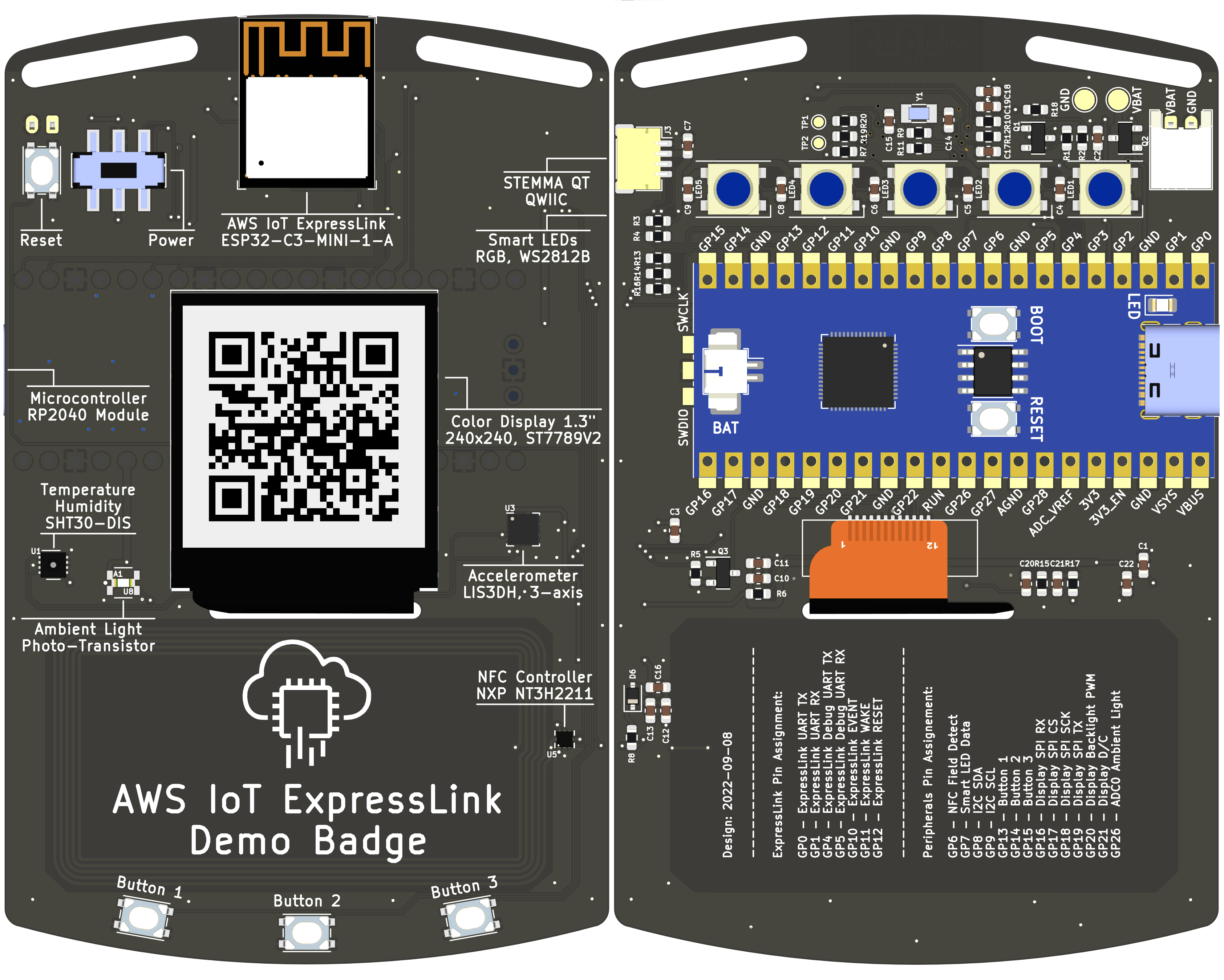
The schematic for the Demo Badge is available as KiCAD 6 project. You can access a PDF version of the single-sheet schematic here.
The PCB layout for the Demo Badge is available as KiCAD 6 project, including all footprints (publicly available ones, and custom ones).
You can access the production Gerber files here.
If you made any changes to the PCB layout, you have to re-generate the Gerbers files before sending them to your PCB manufacturer. You can use KiBot to generate Gerbers and other files in a repeatable way using the kibot.yaml configuration file.
You can follow the KiBot installation guide, or use a Docker container:
docker run --rm -v "$PWD":/kicad -w /kicad setsoft/kicad_auto:ki6 kibot -c kibot.yamlAll KiBot-generated files are available under Generated/.
This hardware design is licensed under the MIT-0 License. Imported footprints and 3D models might contain different licenses.
| Qty | Value | Footprint | References |
|---|---|---|---|
| 12 | 10k | Resistor_SMD:R_0603_1608Metric | R5, R7, R8, R10, R12, R13, R14, R15, R16, R18, R19, R20 |
| 10 | 100n | Capacitor_SMD:C_0603_1608Metric | C1, C2, C3, C10, C12, C13, C16, C17, C18, C22 |
| 8 | 1u | Capacitor_SMD:C_0603_1608Metric | C4, C5, C6, C8, C9, C11, C20, C21 |
| 5 | WS2812B | reinvent-2022-expresslink-badge:SK6812-multi | D1, D2, D3, D4, D5 |
| 4 | 1k | Resistor_SMD:R_0603_1608Metric | R1, R2, R11, R17 |
| 4 | PTS815_SJM_250_SMTR_LFS | PTS815:PTS815 SJM 250 SMTR LFS | SW1, SW3, SW4, SW5 |
| 2 | 10u | Capacitor_SMD:C_0603_1608Metric | C7, C19 |
| 2 | 27pf | Capacitor_SMD:C_0603_1608Metric | C14, C15 |
| 2 | 2N7002 | Package_TO_SOT_SMD:SOT-23 | Q1, Q3 |
| 2 | 4k7 | Resistor_SMD:R_0603_1608Metric | R3, R4 |
| 2 | MountingHole | reinvent-2022-expresslink-badge:lanyard-cutout | H1, H2 |
| 2 | TestPoint | TestPoint:TestPoint_Pad_D1.0mm | TP1, TP2 |
| 1 | 1N5819WS | Diode_SMD:D_SOD-323 | D6 |
| 1 | 7.5 | Resistor_SMD:R_0603_1608Metric | R6 |
| 1 | ALS-PT19-315C/L177/TR8 | ALS-PT19-315C_L177_TR8:XDCR_ALS-PT19-315C_L177_TR8 | A1 |
| 1 | BATT_NEG | TestPoint:TestPoint_Pad_D2.0mm | J1 |
| 1 | BATT_POS | TestPoint:TestPoint_Pad_D2.0mm | J2 |
| 1 | Crystal | Crystal:Crystal_SMD_3215-2Pin_3.2x1.5mm | Y1 |
| 1 | DMG2305UX-7 | Package_TO_SOT_SMD:SOT-23 | Q2 |
| 1 | DNP | Resistor_SMD:R_0603_1608Metric | R9 |
| 1 | ER-TFT013-2 | ER-TFT013-2:ER-TFT013-2 | U4 |
| 1 | ESP32-C3-MINI-1-A | Espressif:ESP32-C3-MINI-1 | U7 |
| 1 | IN-S32GTLS | IN-S32GTLS:IN-S32GTLS | U8 |
| 1 | JS202011SCQN | JS2020:JS202011SCQN | SW2 |
| 1 | LIS3DH | Package_LGA:LGA-16_3x3mm_P0.5mm_LayoutBorder3x5y | U3 |
| 1 | LOGO | LOGO | G*** |
| 1 | NT3H2211W0FHKH | NT3H2211W0FHKH:IC_NT3H2211W0FHKH | U5 |
| 1 | QWIIC | Connector_JST:JST_SH_SM04B-SRSS-TB_1x04-1MP_P1.00mm_Horizontal | J3 |
| 1 | SHT30-DIS | Sensor_Humidity:Sensirion_DFN-8-1EP_2.5x2.5mm_P0.5mm_EP1.1x1.7mm | U1 |
| 1 | Waveshare-RP2040-Plus | reinvent-2022-expresslink-badge:Waveshare-RP2040-Plus | U2 |
| 1 | socket-matching-battery-holder-plug | Connector_JST:JST_PH_S2B-PH-K_1x02_P2.00mm_Horizontal | J4 |
It measures 59.2 × 93.2 mm and has 2 copper layers, 1.63 mm thick.
74 parts, built around the IN-S32GTLS, SHT30-DIS, ALS-PT19-315C/L177/TR8 and LIS3DH. The full list of its parts is on this page, with links to each part's symbol and footprint where PCBKit's library has them.
From the aws/iot-expresslink repository on GitHub, at the commit this page was made from: the board is hardware-designs/DemoBadge/aws-iot-expresslink-demo-badge.kicad_pcb and its schematic hardware-designs/DemoBadge/aws-iot-expresslink-demo-badge.kicad_sch. PCBKit opens the board in the browser, with nothing to install.
Its repository publishes it under the MIT-0 licence: you may reuse it on that licence's terms (keep the author's notice, and for a copyleft licence share your changes alike).
aws-samples/aws-iot-connected-product-demo-badge
This device was designed and created for a hands-on workshop at re:Invent 2023.

devinhorowitz/solar-business-card
Front — the card face Back — the component side

EIT-team/sVNS_circular_implant_kicad
KiCad project for sVNS circular formfactor implant

kwame-y/PCBCard
Custom PCB Business card as my first electrical engineering related project (for Hack Club Forge)


chatelao/xDuinoRail-Decoder
The friendly decoder development plattform for model railroad tinkers.

Pegoku/Home-Assistant-Control-pad
This is a programmable Home Assistant Control Pad. It can control 4 Home assistant devices at a time, and has 4 togglable screens/zones (in total 16 devices).

CommanderRedYT/ws2812-clock
A simple pcb clock using ws2812 in 7-segment form