2 layers216 × 70.8 mm
Choc40
rainkeebs/Choc40
40% Low profile keyboard designed for Kailh 'Choc' v1 switches and MBK Extended keycaps.
98 parts15Unlicense

 awkwardbunny/KiPad
Custom PCB + 3D printed keycaps and case.
KiPad is an open-source printed circuit board by awkwardbunny, from the awkwardbunny/KiPad repository on GitHub. It is a 2-layer board of 81.9 × 126.7 mm with 84 parts on 77 nets, routed with 688 tracks and 354 vias.
It is built around the ATMEGA32U2-MU and SK6812MINI-E. Its parts include 42 diodes, 22 switches, 6 capacitors, 5 resistors and 1 IC. It belongs with the AVR (ATmega, ATtiny) boards of this library.


Custom keypad made using KiCad.
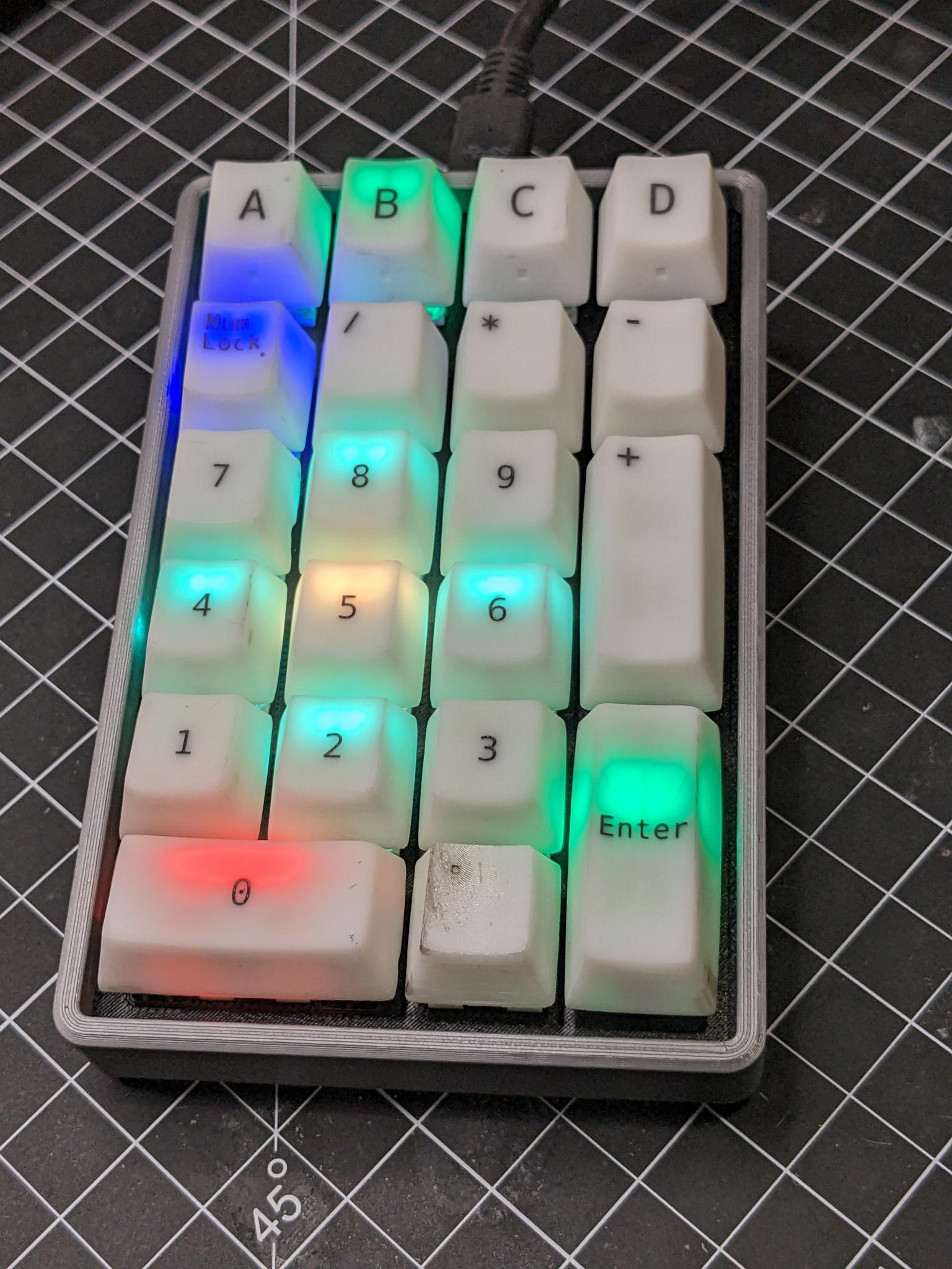
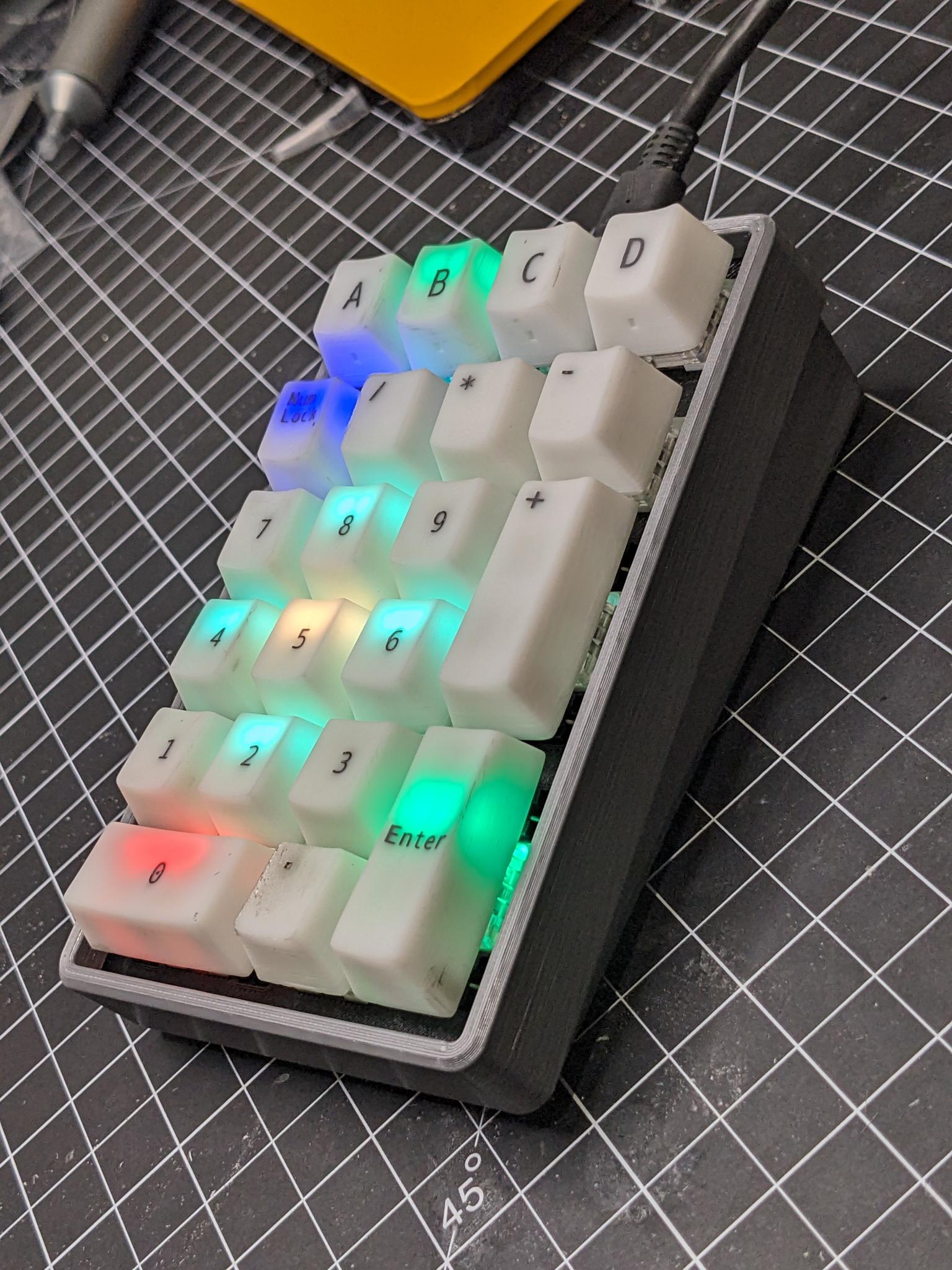
Custom PCB + 3D printed keycaps and case.
The PCB was designed in KiCad and manufactured by JLCPCB.
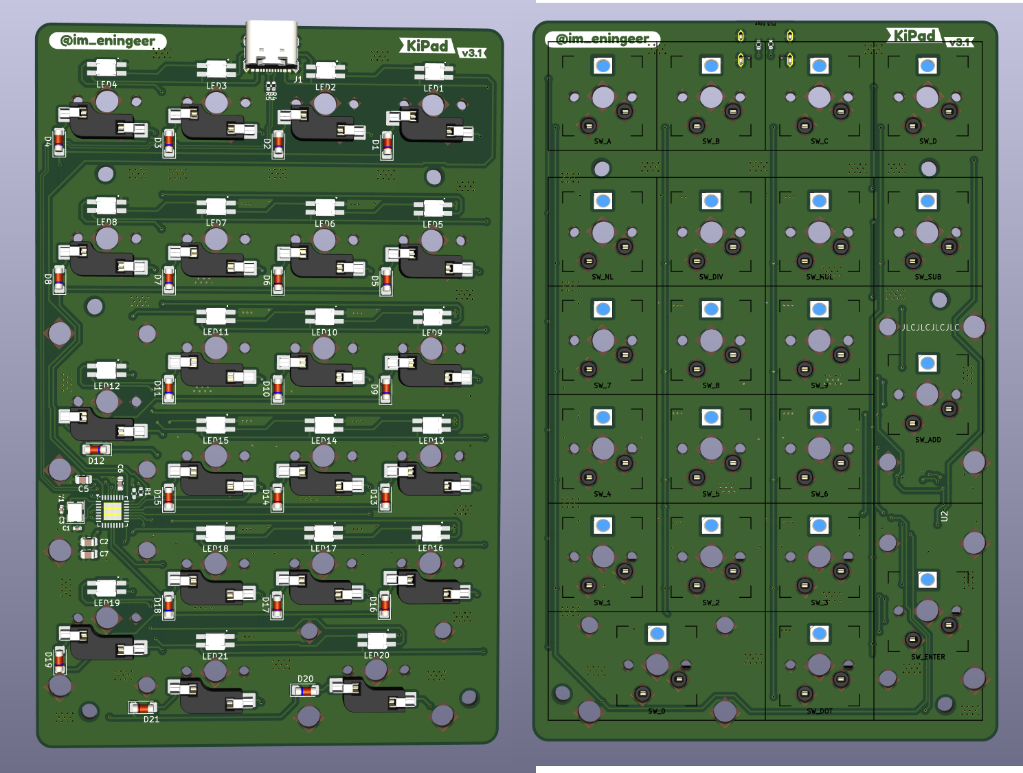
Most of the components have a custom field DIGIKEY, which corresponds to the Digikey part number.
Components can be ordered from Digikey easily by doing a BOM export and using Digikey's upload list feature.
The hotswap connectors, key switches, and stablizers do not have Digikey part numbers. Choose ones you like.
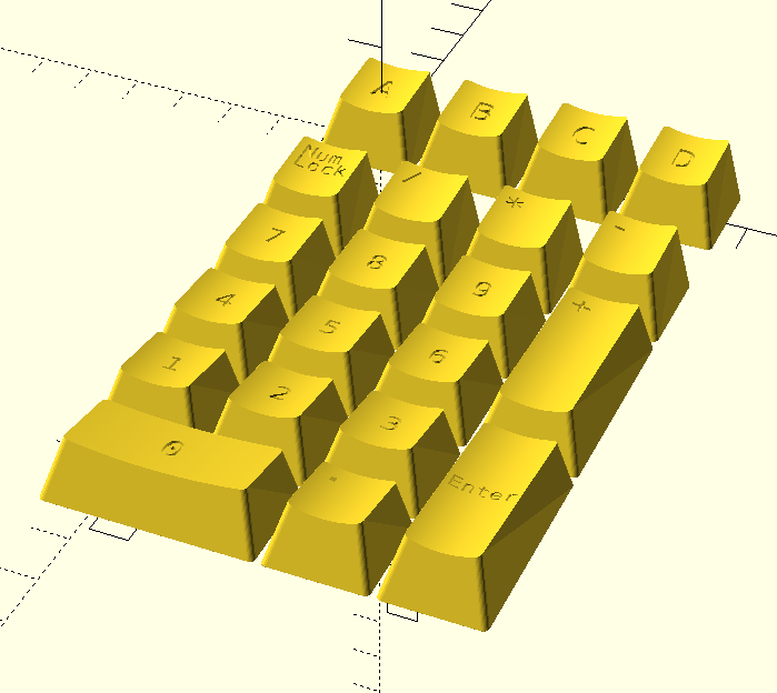
The keycaps were generated using this library.
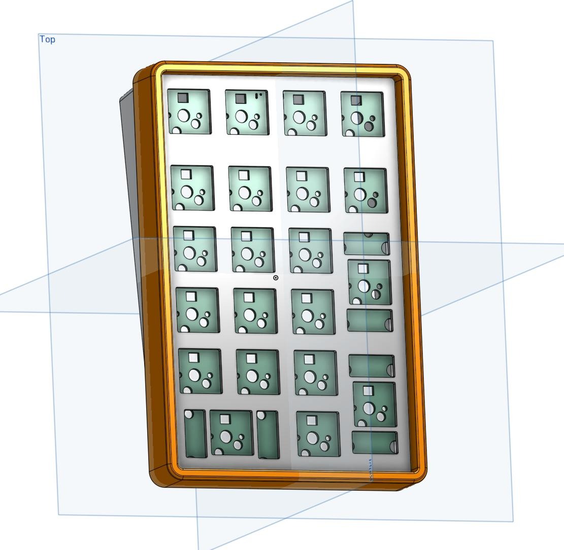
The PCB was exported from KiCad and a case was modeled around it using OnShape. The models can be found under case/ or on OnShape.
The bottom of the case is designed to fit 1.2mm thick boards, so keep that in mind when putting in the PCB order.
To build the firmware, follow the QMK setup, and then copy/link the qmk directory into the keyboards directory:
# Clone project
git clone https://github.com/awkwardbunny/KiPad
cd KiPad
# By default, QMK installs to ~/qmk_firmware on linux
ln -s $(pwd)/qmk ~/qmk_firmware/keyboards/meirl
# Flash. Use the directory name above
qmk flash -kb meirl/kipad_v3_1 -km viaThe Atmega32u2 goes into DFU bootloader without any code on it. If you wish to reflash, connect the keypad while holding down the top-left key (A).
If a bad firmware was uploaded and you cannot get it into DFU mode with that method, you need to trigger a reset while the HWB pin is pulled low.
There is a pad exposed on the back for reset, and the HWB pin is connected to column 3. I solder one wire to each of these and do the following:
And the device should show up in DFU mode
To use with Via, you need to enable Settings -> Show design tab -> Enable. A new tab should appear.
Open the new design tab and upload the keyboard definition qmk/kipad_v3_1/via.json. Now you should be able to reconfigure it as you like.
For linux, Via may not be able to access the keypad HID devices due to permissions. Try adding the following to /etc/udev/rules.d/90-kipad.rules:
# MEIRL KiPad v2.0
SUBSYSTEM=="usb", ATTRS{idVendor}=="4248", ATTRS{idProduct}=="4b50", MODE="0666"
KERNEL=="hidraw*", ATTRS{busnum}=="1", ATTRS{idVendor}=="4248", ATTRS{idProduct}=="4b50", MODE="0666"

# MEIRL KiPad v3.0
SUBSYSTEM=="usb", ATTRS{idVendor}=="4248", ATTRS{idProduct}=="4b51", MODE="0666"
KERNEL=="hidraw*", ATTRS{busnum}=="1", ATTRS{idVendor}=="4248", ATTRS{idProduct}=="4b51", MODE="0666"

# MEIRL KiPad v3.1
SUBSYSTEM=="usb", ATTRS{idVendor}=="4248", ATTRS{idProduct}=="4b52", MODE="0666"
KERNEL=="hidraw*", ATTRS{busnum}=="1", ATTRS{idVendor}=="4248", ATTRS{idProduct}=="4b52", MODE="0666"
And then sudo udevadm control --reload.
| Qty | Value | Footprint | References |
|---|---|---|---|
| 21 | SK6812MINI | Custom:LED_SK6812MINI-E_PLCC4_3.2x2.8mm_P1.75mm | LED1, LED2, LED3, LED4, LED10, LED11, LED12, LED13, LED14, LED15, LED16, LED17, LED18, LED19, LED20, LED21 +5 |
| 21 | ~ | Diode_SMD:D_MiniMELF | D1, D2, D3, D4, D10, D11, D12, D13, D14, D15, D16, D17, D18, D19, D20, D21 +5 |
| 2 | 0.1u | Capacitor_SMD:C_0805_2012Metric | C2, C5 |
| 2 | 22 | Resistor_SMD:R_0402_1005Metric | R4, R5 |
| 2 | 22p | Capacitor_SMD:C_0402_1005Metric | C1, C3 |
| 2 | 5.1k | Resistor_SMD:R_0402_1005Metric | R2, R3 |
| 2 | G*** | kibuzzard-66A8A61F | kibuzzard-66A8A61F, kibuzzard-66A8A61F |
| 2 | G*** | kibuzzard-66A8A670 | kibuzzard-66A8A670, kibuzzard-66A8A670 |
| 2 | G*** | kibuzzard-66A8A64C | kibuzzard-66A8A64C, kibuzzard-66A8A64C |
| 1 | 10k | Resistor_SMD:R_0402_1005Metric | R1 |
| 1 | 10u | Capacitor_SMD:C_0805_2012Metric | C7 |
| 1 | 16MHz | Crystal:Crystal_SMD_3225-4Pin_3.2x2.5mm | Y1 |
| 1 | 1u | Capacitor_SMD:C_0603_1608Metric | C6 |
| 1 | ATmega32U2-M | Package_DFN_QFN:QFN-32-1EP_5x5mm_P0.5mm_EP3.1x3.1mm | U2 |
| 1 | RESET | Resistor_SMD:R_0402_1005Metric_Pad0.72x0.64mm_HandSolder | SW22 |
| 1 | SW_0 | MX_Hotswap:MX-Hotswap-2U-ReversedStabilizers | SW20 |
| 1 | SW_1 | MX_Hotswap:MX-Hotswap-1U | SW16 |
| 1 | SW_2 | MX_Hotswap:MX-Hotswap-1U | SW17 |
| 1 | SW_3 | MX_Hotswap:MX-Hotswap-1U | SW18 |
| 1 | SW_4 | MX_Hotswap:MX-Hotswap-1U | SW13 |
| 1 | SW_5 | MX_Hotswap:MX-Hotswap-1U | SW14 |
| 1 | SW_6 | MX_Hotswap:MX-Hotswap-1U | SW15 |
| 1 | SW_7 | MX_Hotswap:MX-Hotswap-1U | SW9 |
| 1 | SW_8 | MX_Hotswap:MX-Hotswap-1U | SW10 |
| 1 | SW_9 | MX_Hotswap:MX-Hotswap-1U | SW11 |
| 1 | SW_A | MX_Hotswap:MX-Hotswap-1U | SW1 |
| 1 | SW_ADD | MX_Hotswap:MX-Hotswap-2U-Vertical | SW12 |
| 1 | SW_B | MX_Hotswap:MX-Hotswap-1U | SW2 |
| 1 | SW_C | MX_Hotswap:MX-Hotswap-1U | SW3 |
| 1 | SW_D | MX_Hotswap:MX-Hotswap-1U | SW4 |
| 1 | SW_DIV | MX_Hotswap:MX-Hotswap-1U | SW6 |
| 1 | SW_DOT | MX_Hotswap:MX-Hotswap-1U | SW21 |
| 1 | SW_ENTER | MX_Hotswap:MX-Hotswap-2U-Vertical | SW19 |
| 1 | SW_MUL | MX_Hotswap:MX-Hotswap-1U | SW7 |
| 1 | SW_NL | MX_Hotswap:MX-Hotswap-1U | SW5 |
| 1 | SW_SUB | MX_Hotswap:MX-Hotswap-1U | SW8 |
| 1 | USB_C_Receptacle_USB2.0_14P | Connector_USB:USB_C_Receptacle_GCT_USB4105-xx-A_16P_TopMnt_Horizontal | J1 |
rainkeebs/Choc40
40% Low profile keyboard designed for Kailh 'Choc' v1 switches and MBK Extended keycaps.


bennettzug/binarykb
simple 2 key macropad with USB-C connector and hotswappable switches


It measures 81.9 × 126.7 mm and has 2 copper layers, 1.2 mm thick.
84 parts, built around the ATMEGA32U2-MU and SK6812MINI-E. The full list of its parts is on this page, with links to each part's symbol and footprint where PCBKit's library has them.
From the awkwardbunny/KiPad repository on GitHub, at the commit this page was made from: the board is KiPad.kicad_pcb and its schematic KiPad.kicad_sch. PCBKit opens the board in the browser, with nothing to install.
Its repository states no licence, so its author keeps all rights: ask awkwardbunny before reusing the design.