4 layers25 × 35 mm
Qfn csi underpad diff
drandyhaas/KiCadRoutingTools
A set of Python/Rust tools to aid routing in KiCad
2 parts744MIT

 atuzlak/kicad-splitplane2
Split a KiCad power layer into one continuous copper zone per voltage
Demo board is an open-source printed circuit board by atuzlak, from the atuzlak/kicad-splitplane repository on GitHub, published under the MIT licence. It is a 4-layer board of 80 × 55 mm with 2 parts on 4 nets.
Split a KiCad power layer into exactly one continuous copper zone per voltage, computed from where your vias are.
Available in KiCad's official Plugin and Content Manager: search for kicad-splitplane and press Install (listing).
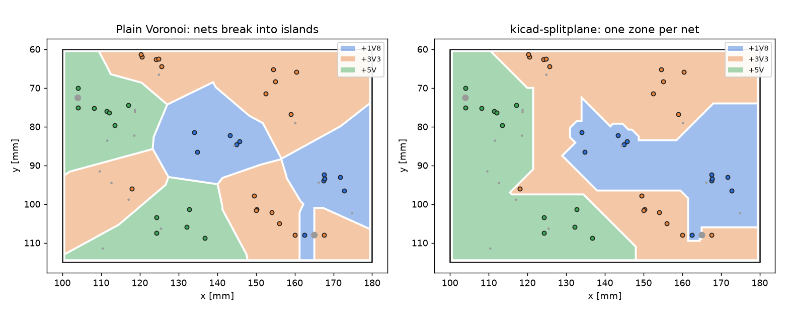
On a 4-layer board the inner power layer is often shared by several supplies (5V, 3.3V, 1.8V…). Each supply needs its own zone, and each zone has to
Drawing those outlines by hand is trial and error. kicad-splitplane does it for you and writes the zones straight into a copy of your .kicad_pcb.
git clone https://github.com/atuzlak/kicad-splitplane
cd kicad-splitplane
pip install -r requirements.txt        # shapely>=2.0, numpy, scipy, matplotlib

python kicad_splitplane.py examples/demo_board.kicad_pcb --nets +5V +3V3 +1V8
On your own board:
python kicad_splitplane.py board.kicad_pcb --list-nets                      # find the supply nets
python kicad_splitplane.py board.kicad_pcb --layer In2.Cu --nets 5V 3.3V VBUS
This writes board_splitplane.kicad_pcb (your board plus the zones; the original is untouched), board_splitplane.png (preview) and a copy of the project files (board_splitplane.kicad_pro/.kicad_prl) that keeps your design rules and shows every zone in its preview colour. Open the new board in KiCad, press B to fill the zones and run DRC.
Or install it as a command:
pip install git+https://github.com/atuzlak/kicad-splitplane
kicad-splitplane board.kicad_pcb --nets 5V 3.3V VBUSThe same tool also runs inside the PCB editor (KiCad 9 or newer). It works on the open board, shows a preview and writes the zones directly into the board as one undo step, so Ctrl+Z removes them again.
kicad-splitplane-<version>-pcm.zip from the releases and use Install from File… (uninstall a zip-installed copy before installing from the list, so updates work).
KiCad installs the Python dependencies on first use, which takes a minute.The dialog has the same options as the command line. It uses the wxPython that ships with KiCad, so nothing else needs to be installed.
For development, link the folder into KiCad's plugin directory instead of installing the zip (e.g. ~/.local/share/kicad/10.0/plugins/, or ~/.var/app/org.kicad.KiCad/data/kicad/10.0/plugins/ for the Flatpak; a Flatpak cannot follow a symlink, so copy the folder together with kicad_splitplane.py there), or run python plugin/splitplane_action.py while KiCad has a board open.
| Option | Default | Meaning |
|---|---|---|
--layer | In2.Cu | Copper layer to split |
--nets | Supply nets that share the layer | |
--list-nets | Print supply-like nets with their via / SMD pad counts | |
--gap | 0.5 mm | Copper gap between neighbouring zones |
--edge | 0.5 mm | Clearance to the board edge |
--min-neck | 1.0 mm | Warn where a zone gets narrower than this |
--res | 0.5 mm | Routing grid. If a via gets trapped, try 0.3–0.6 |
--include-smd | off | Treat SMD pads as vias: preview before you place the power vias |
--no-smooth | off | Keep the raw grid outlines instead of smooth 0°/45°/90° edges |
--plain | off | Skip connecting the vias (faster, may create islands) |
--keep-old | off | Keep existing zones of these nets on the layer (default: replaced) |
--no-colors | off | Don't colour the nets in the copied project file |
--out | <board>_splitplane.kicad_pcb | Output file |
Exit code is 0 when every net got one clean zone, 1 when there are warnings.
--min-neck and prefer the middle of free space. All routing orders of the nets are tried; the one with the fewest trapped vias and the shortest spines wins.--min-neck.If a via is completely enclosed by other nets, no continuous split exists. The tool reports it and suggests where to move it:
! 5V: via at (87.59, 56.06) is trapped by other nets -> move it to ~(92.60, 65.46) (10.6 mm fanout)import kicad_splitplane as sp
text = open("board.kicad_pcb", encoding="utf-8").read()
r = sp.process(text, "In2.Cu", ["5V", "3.3V", "VBUS"], gap=0.5)
print("\n".join(r.log))
open("board_split.kicad_pcb", "w").write(r.board_text)
sp.render_png(r, "preview.png")web/ contains the documentation page; python web/make_figures.py renders its figures. ./deploy.sh builds it as one self-contained file (dist/kicad-splitplane.html), ./deploy.sh --serve previews it locally, ./deploy.sh user@host:public_html uploads it.
python -m pytest tests/ # plugin tests run when kicad-python is installedFound a bug, have an idea for an improvement, or interested in collaborating? Write me an email at atuzlak@ethz.ch. Issues and pull requests are welcome too.
MIT, © 2026 Aleksandar Tuzlak
| Qty | Value | Footprint | References |
|---|---|---|---|
| 1 | — | Connector_PinHeader_2.54mm:PinHeader_1x03_P2.54mm_Vertical | J1 |
| 1 | — | Connector_PinHeader_2.54mm:PinHeader_1x04_P2.54mm_Vertical | J2 |
It measures 80 × 55 mm and has 4 copper layers, 1.6 mm thick.
2 parts. The full list of its parts is on this page, with links to each part's symbol and footprint where PCBKit's library has them.
From the atuzlak/kicad-splitplane repository on GitHub, at the commit this page was made from: the board is examples/demo_board.kicad_pcb. PCBKit opens the board in the browser, with nothing to install.
Its repository publishes it under the MIT licence: you may reuse it on that licence's terms (keep the author's notice, and for a copyleft licence share your changes alike).
drandyhaas/KiCadRoutingTools
A set of Python/Rust tools to aid routing in KiCad


dbalsom/arduinoX86
An interface between an Arduino Due or Arduino GIGA and 8088, 8086, V20, V30, 186 or 286 CPUs

agranlund/raven
Homemade MC68060 + DSP56303 Atari-compatible computer. Hardware, firmware, and software stack


imendizabal/Near-Field-Probes
Open Source kit of Near Field Probes for Electromagnetic Compatibility (EMC) troubleshooting