
2 layers76 × 63.8 mm

 ashlin4010/OmniProbe
PDP-8 Omnibus Logic Probe
OmniProbe is an open-source printed circuit board by ashlin4010, from the ashlin4010/OmniProbe repository on GitHub. It is a 4-layer board of 265.6 × 150.5 mm with 249 parts on 354 nets, routed with 2,283 tracks and 362 vias.
It is built around the 74HCT244D. Its parts include 97 resistors, 96 diodes, 20 capacitors, 16 connectors and 12 ICs. It belongs with the sensors and measurement boards of this library.
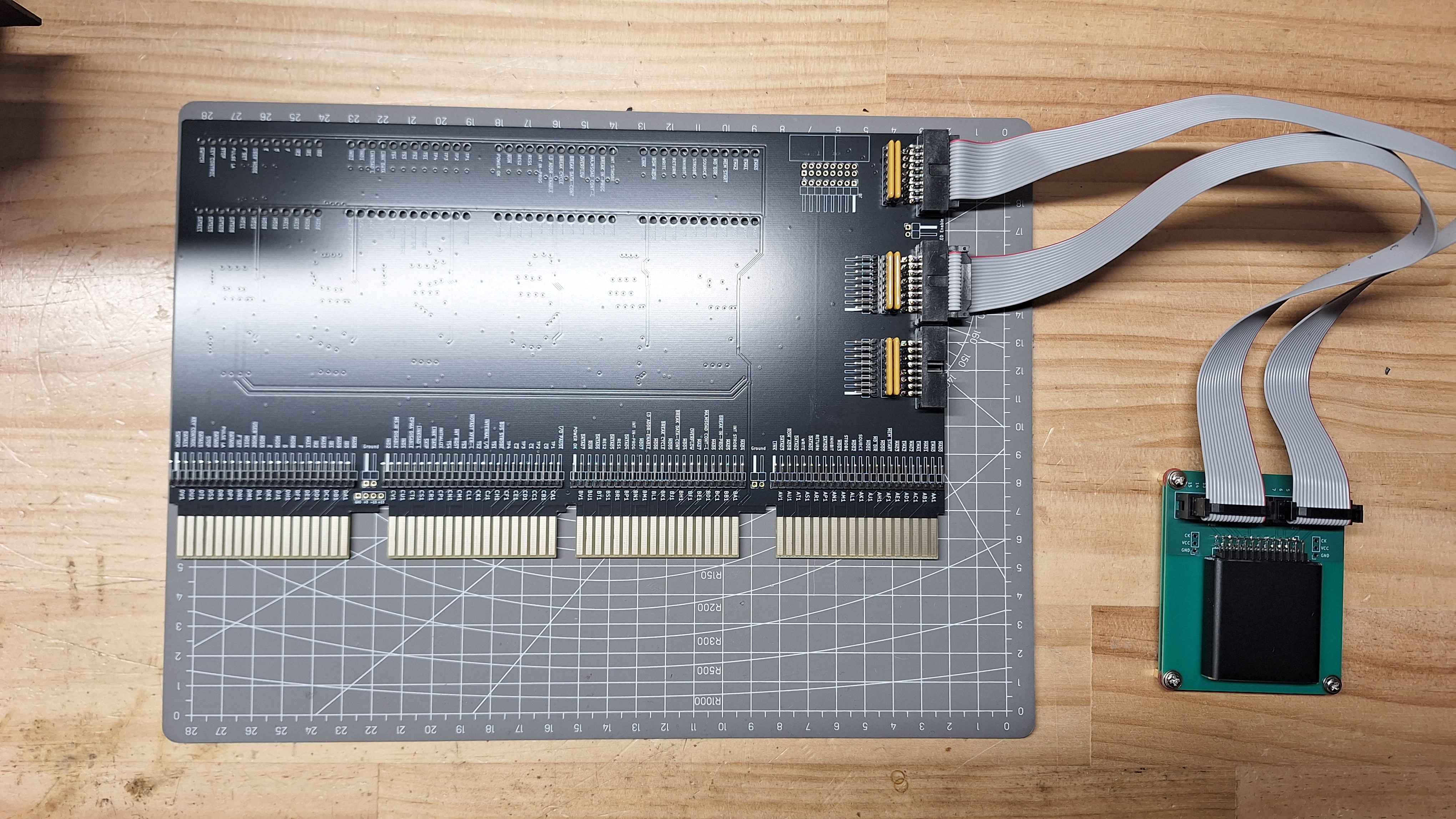
OmniProbe is a basic debugging tool for the PDP-8e. Its main function is to provide a simple interface to connect up a logic analyzer to the PDP-8e's bus. The OmniProbe also provides LEDs for each of the 96 signals that make up the Omnibus, allowing you to see the state of the bus in real time.
The OmniProbe provides up to 24 signals to the logic analyzer, 8 of which have fixed assignments, and 16 of which can be assigned to any of the 96 signals on the Omnibus. Additionally, there is a connector along the top edge of the board that allows you to connect up the logic analyzer to the top edge of omnibus cards.
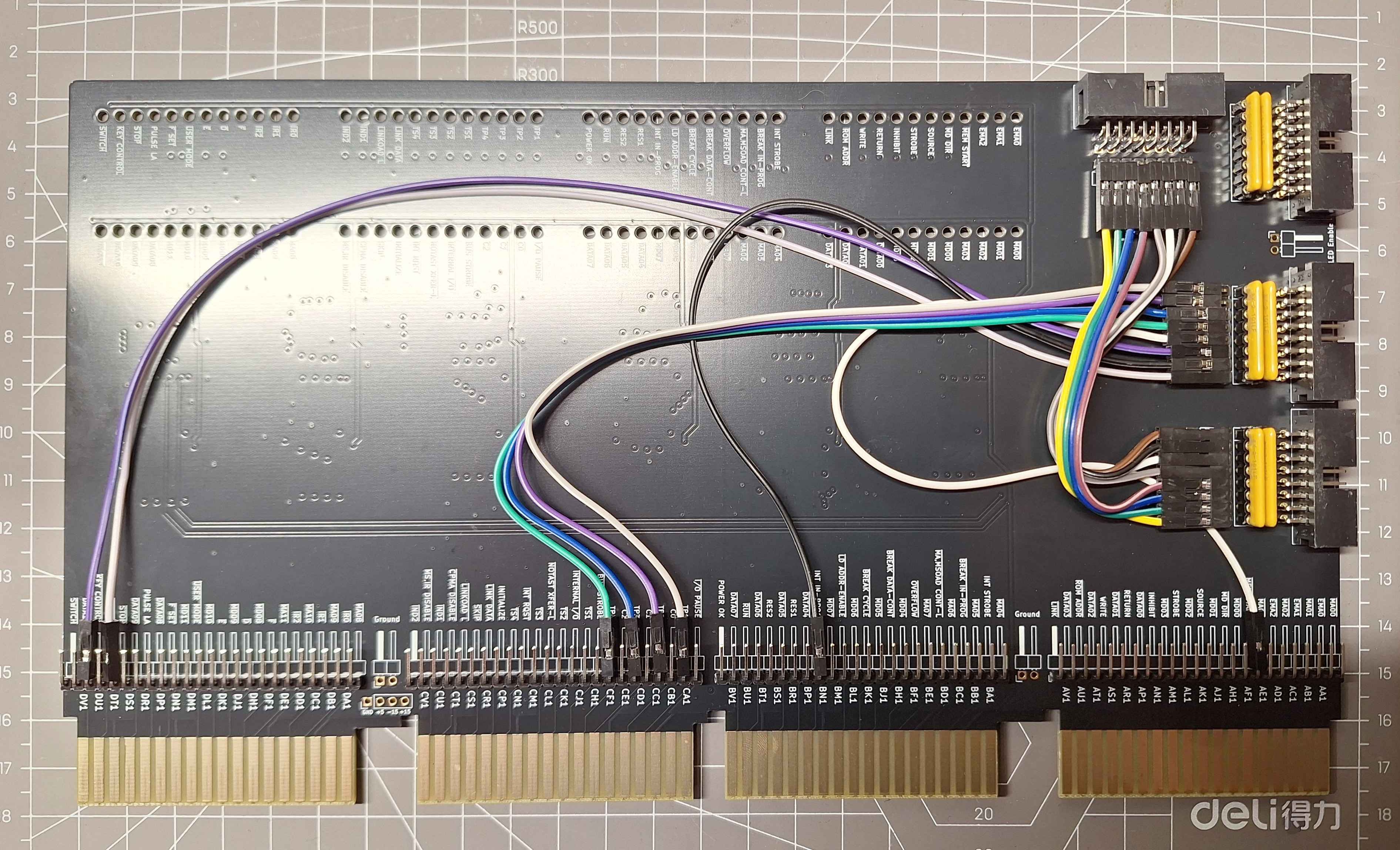
The OmniProbe is designed to be compatible with the PDP-8e Omnibus. It has not been tested or designed to be compatible with any other PDP-8 model. Use at your own risk. If building for the PDP-8/A I recommend using straight Box headers to connectors to ensure that you have clearance for the card to fit into the system.
Let me know if you have any issues with the design or have tested it with other PDP-8 models.
See fabrication.
A large portion of the OmniProbe design is based on the UniProbe and UniBone design by Jörg Hoppe. This included the some PCB footprints and general design. This design is released under the same license as the UniBone, which is the CERN Open Hardware Licence Version 2 - Permissive.
See the LICENSE file for more information.
The OmniProbe is designed to be installed in a PDP-8e Omnibus card slot. I recommend making two boards, one populated with the LEDs and drivers. The second board should be populated with the connectors and the logic analyzer interface.
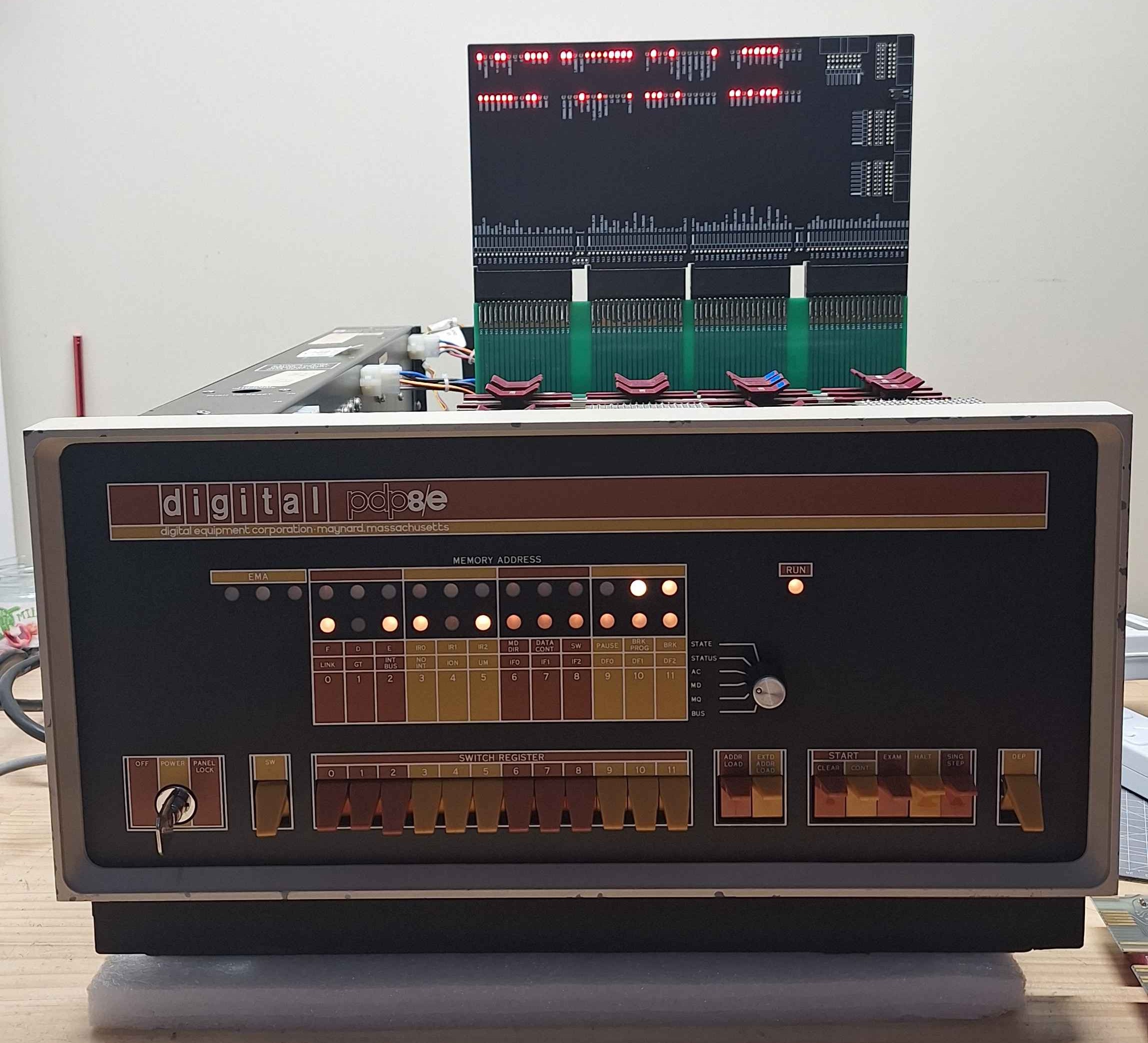
The board with the LEDs is best viewed when installed on an riser card, so that the LEDs are visible from the front of the PDP-8e. The second board can be installed in any Omnibus, where ever is convenient.
Fixed assignments are as follows: RUN, TS1, TS2, TS3, TS4, F, D, and E.
Omnibus cards have a set of fingers along the top edge that are used to connect between cards. These fingers are not connected to the Omnibus, but they can be connected to the logic analyzer via the OmniProbe. The OmniProbe has a connector along the top edge to accommodate this. Note that half of the pins on the top edge connector can be connected to ground via a solder jumper. To avoid any issues, I recommend putting jumpers over the ground pins to prevent any accidental shorts.
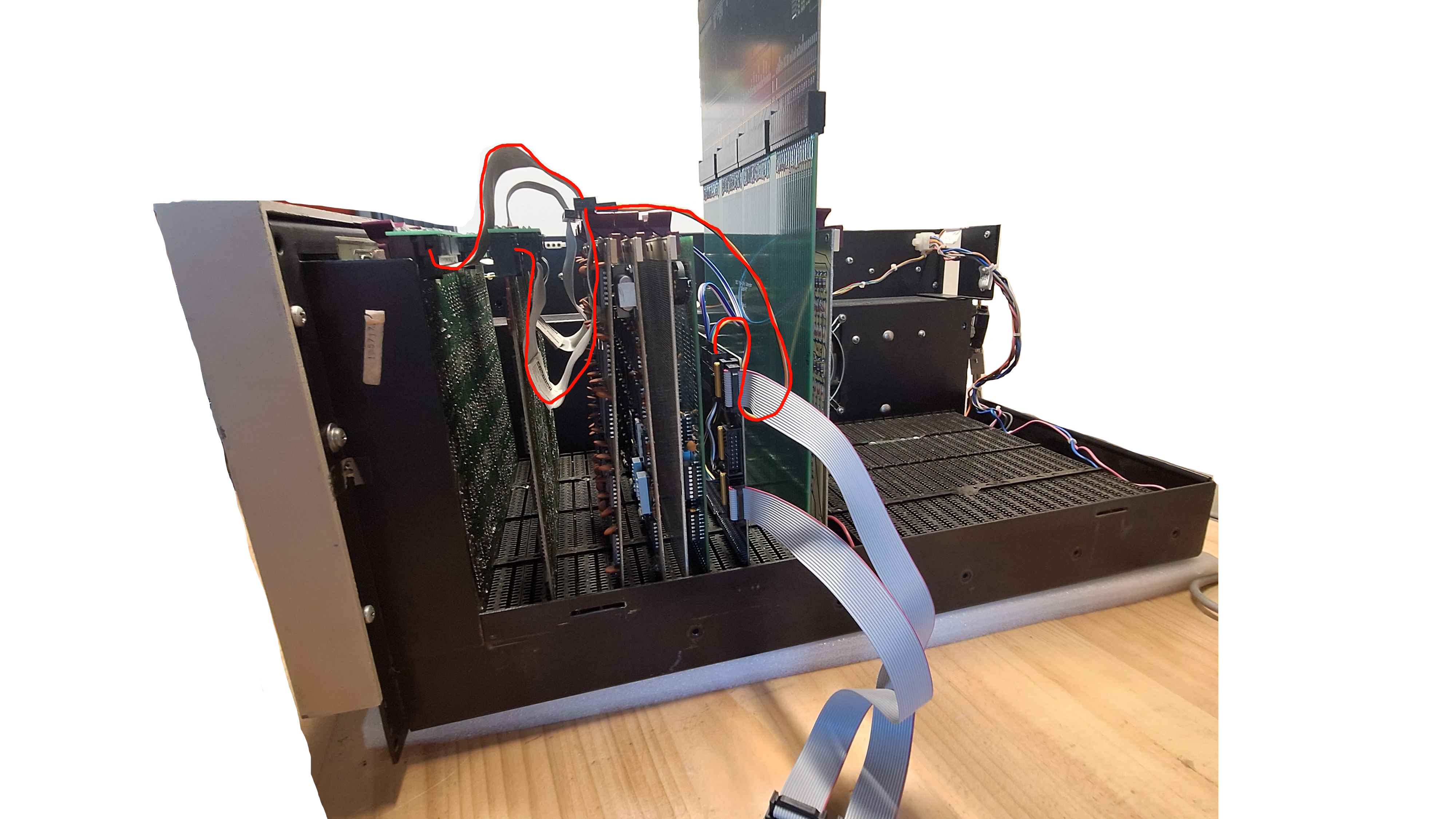
I recommend building up a set of H851 extension cables. They have two functions. First, they allow you to connect Omnibus cards together while one is install on a riser card. Second, they allow you to connect the OmniProbe by tapping the signals off from the ribbon cable.
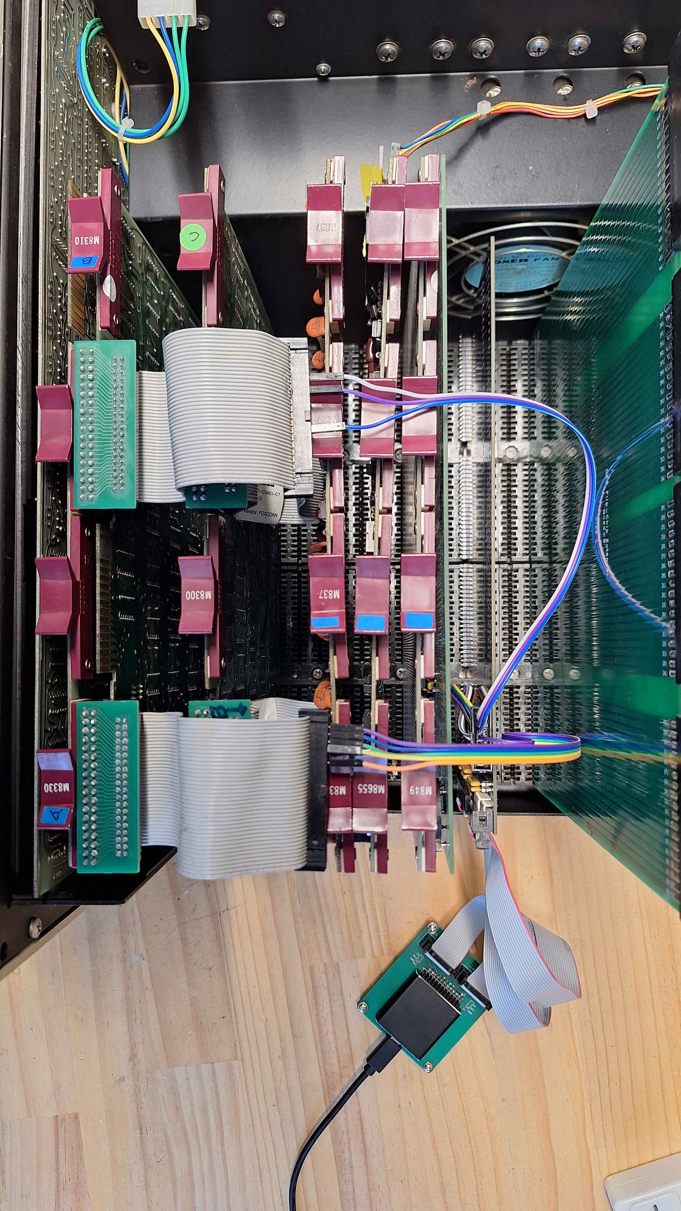
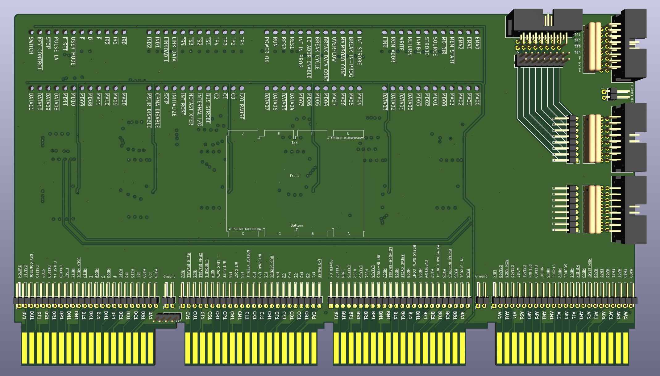
In the folder SLogic_pod you will find a PCB that will allow you to connect a SLogic logic analyzer with out needing to fuss with and cables.
| Qty | Value | Footprint | References |
|---|---|---|---|
| 97 | 4k7 | Resistor_SMD:R_0805_2012Metric_Pad1.20x1.40mm_HandSolder | R1, R2, R10, R11, R12, R13, R14, R15, R16, R17, R18, R19, R20, R21, R22, R23 +81 |
| 96 | LED_Small | local:LED_Osram_Lx_P47F_D2mm_ReverseMount_hand_solder | D1, D2, D10, D11, D12, D13, D14, D15, D16, D17, D18, D19, D20, D21, D22, D23 +80 |
| 20 | 100nF 50V | Capacitor_SMD:C_0805_2012Metric_Pad1.18x1.45mm_HandSolder | C1, C2, C3, C4, C5, C10, C11, C12, C13, C14, C15, C16, C17, C18, C19, C20 +4 |
| 12 | 74HCT244 | Package_SO:SOIC-20W_7.5x12.8mm_P1.27mm | U1, U2, U3, U4, U5, U6, U7, U8, U9, U10, U11, U12 |
| 6 | R_Pack04_Even_odd | Resistor_THT:R_Array_SIP8 | RN1, RN2, RN3, RN4, RN5, RN6 |
| 2 | Ground | Connector_PinHeader_2.54mm:PinHeader_1x02_P2.54mm_Horizontal | J10, J15 |
| 2 | POD_1_PINS | Connector_PinHeader_2.54mm:PinHeader_1x08_P2.54mm_Horizontal | J6, J7 |
| 2 | POD_GROUND | Jumper:SolderJumper-2_P1.3mm_Open_RoundedPad1.0x1.5mm | GND, JP2 |
| 1 | CONN-DEC-QUAD-ABCD | local:dec-conn-quad-pin-only | J1 |
| 1 | Conn_01x02_Pin | Connector_PinHeader_2.54mm:PinHeader_1x02_P2.54mm_Horizontal | J9 |
| 1 | Conn_02x08_Odd_Even | Connector_PinHeader_2.54mm:PinHeader_2x08_P2.54mm_Vertical | J17 |
| 1 | Edge_A | Connector_PinHeader_2.54mm:PinHeader_1x24_P2.54mm_Horizontal | J11 |
| 1 | Edge_B | Connector_PinHeader_2.54mm:PinHeader_1x24_P2.54mm_Horizontal | J12 |
| 1 | Edge_C | Connector_PinHeader_2.54mm:PinHeader_1x24_P2.54mm_Horizontal | J13 |
| 1 | Edge_D | Connector_PinHeader_2.54mm:PinHeader_1x24_P2.54mm_Horizontal | J14 |
| 1 | POD_1 | Connector_IDC:IDC-Header_2x08_P2.54mm_Horizontal | J3 |
| 1 | POD_2 | Connector_IDC:IDC-Header_2x08_P2.54mm_Horizontal | J4 |
| 1 | POD_FIXED | Connector_IDC:IDC-Header_2x08_P2.54mm_Horizontal | J2 |
| 1 | POD_FLYING | Connector_IDC:IDC-Header_2x08_P2.54mm_Horizontal | J5 |
| 1 | Power | Connector_PinHeader_2.54mm:PinHeader_1x04_P2.54mm_Vertical | J16 |


schlae/snark-barker-mca
A Sound Blaster compatible sound card for Micro Channel bus computers

artemisamsx/artemisa
Schematics, PCB designs and HDL simulations to build a 8-bits MSX computer

istedman/A600Reborn
Amiga A600 schematics recpatured in KiCad and a new PCB design from them. Base version


jtsiomb/emurom
ROM emulator. Accepts ROM images through USB and acts as a parallel ROM chip.
It measures 265.6 × 150.5 mm and has 4 copper layers, 1.6 mm thick.
249 parts, built around the 74HCT244D. The full list of its parts is on this page, with links to each part's symbol and footprint where PCBKit's library has them.
From the ashlin4010/OmniProbe repository on GitHub, at the commit this page was made from: the board is OmniProbe.kicad_pcb and its schematic OmniProbe.kicad_sch. PCBKit opens the board in the browser, with nothing to install.
Its repository states no licence, so its author keeps all rights: ask ashlin4010 before reusing the design.