Skip to the content
PCBKitNew board
2 layers37 × 75 mmDevboard, the printed circuit board in 3D

Devboard

arnv15/Helix

Custom Devboard

Size
37 × 75 mm
Copper layers
2
Thickness
1.6 mm
Parts
49
Nets
71
Pads
260
Tracks, vias
437, 28
Pours
1
Routed
Yes
KiCad
KiCad 9.0 (file 20241229)
Created
4 Jun 2026
Updated
16 Jul 2026

Overview

Devboard is an open-source printed circuit board by arnv15, from the arnv15/Helix repository on GitHub. It is a 2-layer board of 37 × 75 mm with 49 parts on 71 nets, routed with 437 tracks and 28 vias.

It is built around the RP2040, ESP32-C3-WROOM-02-H4 and W25Q128JVSIQ, with the AP2112K-3.3TRG1 and SK6812MINI-E among its other parts. Its parts include 20 capacitors, 9 resistors, 5 connectors, 4 ICs and 4 switches. It belongs with the microcontroller boards boards and the ESP32, RP2040 and RISC-V boards of this library.

Main components

5

README

README.md

Helix

My take on an Arduino — a custom development board built around the Raspberry Pi RP2040, designed from schematic through to a fully routed, manufacturable PCB.

About the Project

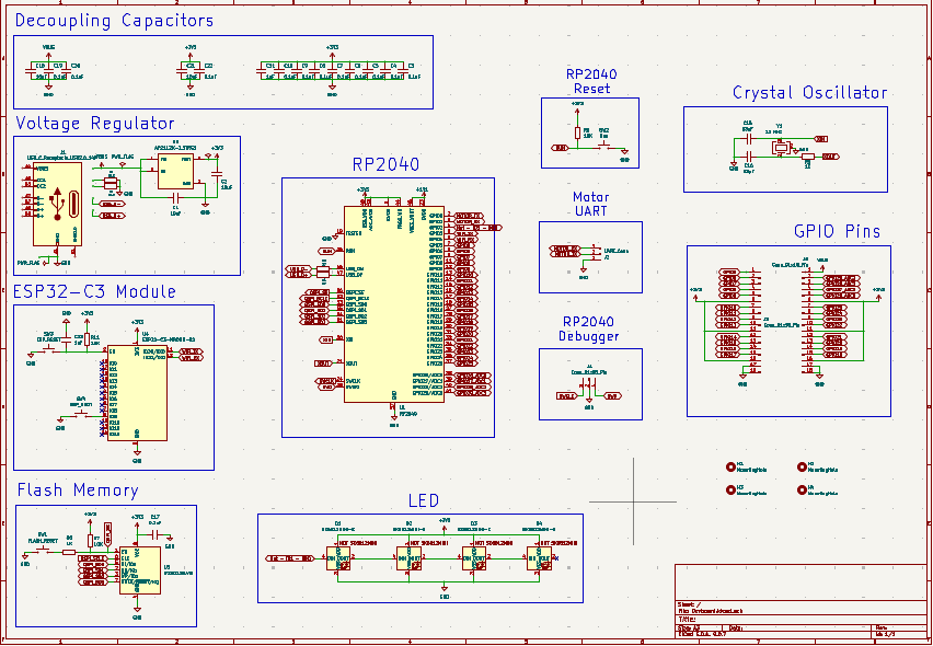
Helix is a hand-designed development board built to learn the fundamentals of circuit design. It's built around a full RP2040 microcontroller, with a voltage regulator, USB-C connector, crystal oscillator, external flash memory, two rows of GPIO pins (ESP-style, breadboard-friendly), and external UART pins for connecting to a motor controller.

The longer-term goal of the project is to use Helix as the MCU for an SO-101 robotic arm, which is controlled over a UART connection.

See JOURNAL.md for the full build log, including design decisions, DRC fixes, and lessons learned along the way.

Build Progress

Designing the schematic
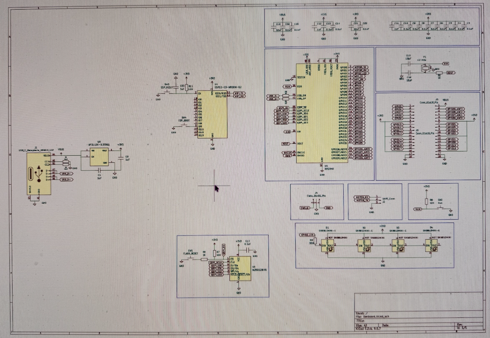
Schematic layout

Finished schematic design

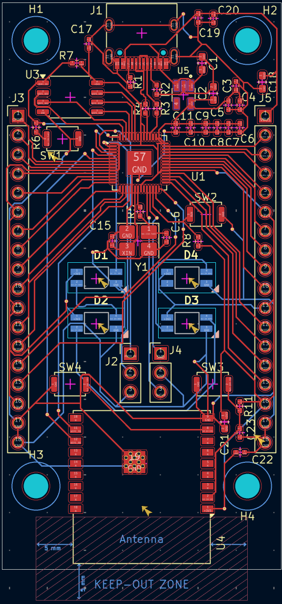
Schematic layout

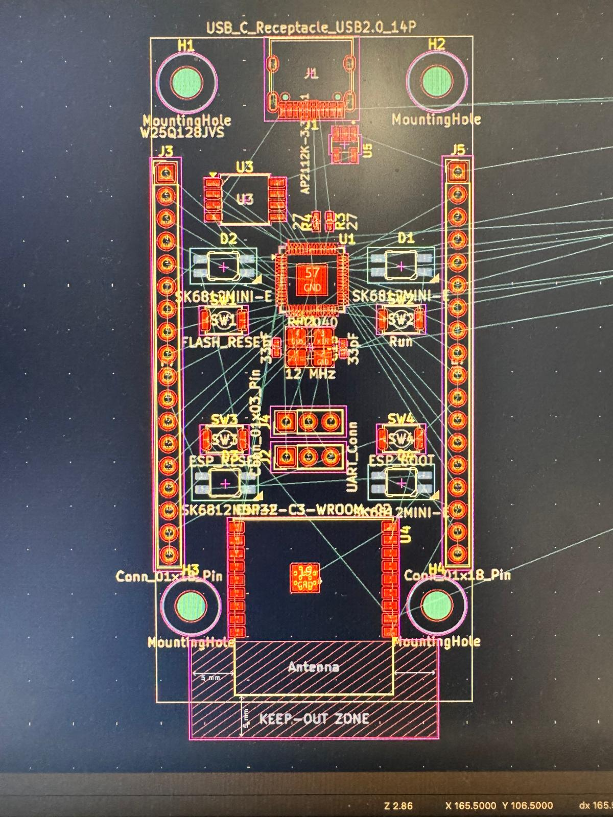
Starting the PCB layout

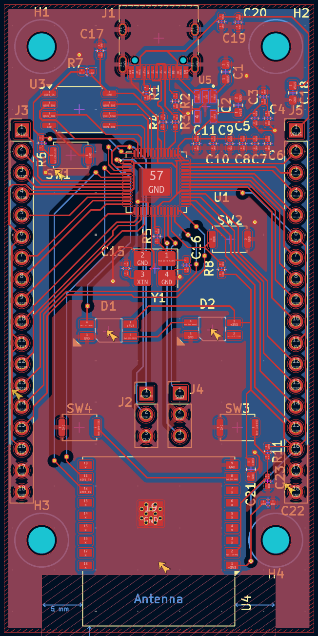
PCB layout

Routing the main components
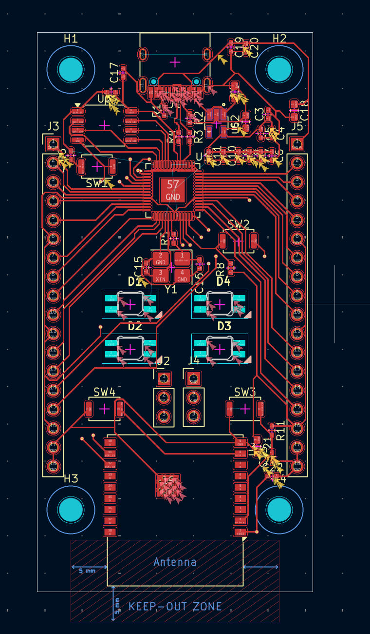
PCB layout

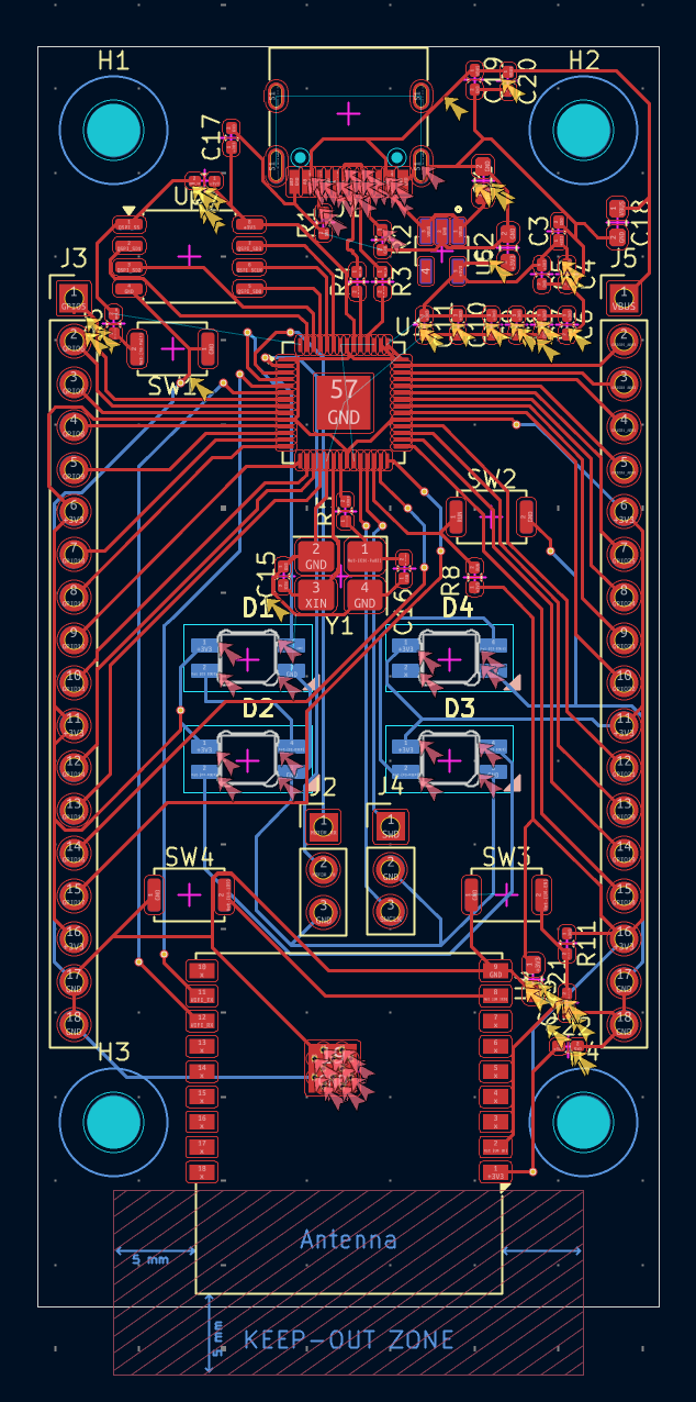
Finished routing both layers

PCB layout

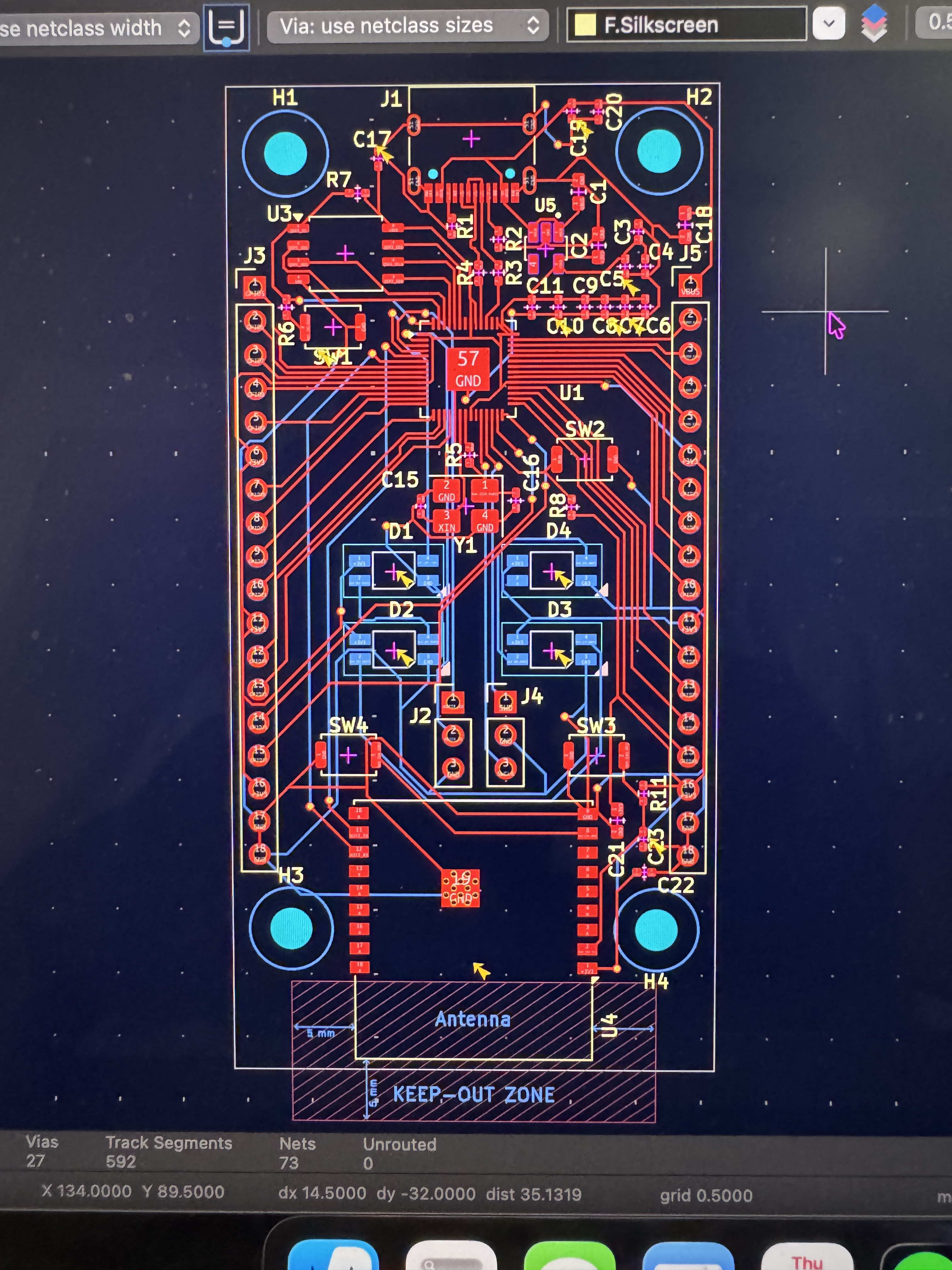
Fixing DRC errors

PCB layout

Cleaning up silkscreen and warnings

PCB layout

Adding a filled ground zone

PCB layout

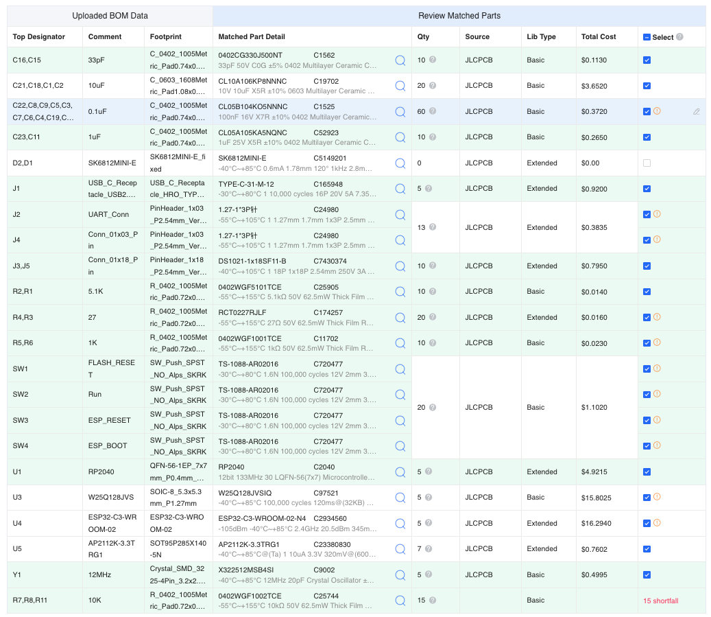
Part selection and BOM

BOM

Bill of Materials

Parts were sourced using the BOM below, with manufacturing and assembly done through JLCPCB (many of the components are too small to hand-solder without a hot plate).

DesignatorFootprintQtyComment
C22,C8,C9,C5,C3,C7,C6,C4,C19,C10,C17,C20C_0402_1005Metric_Pad0.74x0.62mm_HandSolder120.1uF
J3,J5PinHeader_1x18_P2.54mm_Vertical2Conn_01x18_Pin
U3SOIC-8_5.3x5.3mm_P1.27mm1W25Q128JVS
R2,R1R_0402_1005Metric_Pad0.72x0.64mm_HandSolder25.1K
Y1Crystal_SMD_3225-4Pin_3.2x2.5mm_HandSoldering112 MHz
C21,C18,C1,C2C_0603_1608Metric_Pad1.08x0.95mm_HandSolder410uF
SW4SW_Push_SPST_NO_Alps_SKRK1ESP_BOOT
R5,R6R_0402_1005Metric_Pad0.72x0.64mm_HandSolder21K
U5SOT95P285X140-5N1AP2112K-3.3TRG1
J4PinHeader_1x03_P2.54mm_Vertical1Conn_01x03_Pin
R4,R3R_0402_1005Metric_Pad0.72x0.64mm_HandSolder227
C16,C15C_0402_1005Metric_Pad0.74x0.62mm_HandSolder233pF
U4ESP32-C3-WROOM-021ESP32-C3-WROOM-02
SW3SW_Push_SPST_NO_Alps_SKRK1ESP_RESET
R7,R8,R11R_0402_1005Metric_Pad0.72x0.64mm_HandSolder310K
J2PinHeader_1x03_P2.54mm_Vertical1UART_Conn
C23,C11C_0402_1005Metric_Pad0.74x0.62mm_HandSolder21uF
SW2SW_Push_SPST_NO_Alps_SKRK1Run
U1QFN-56-1EP_7x7mm_P0.4mm_EP3.2x3.2mm1RP2040
SW1SW_Push_SPST_NO_Alps_SKRK1FLASH_RESET
J1USB_C_Receptacle_HRO_TYPE-C-31-M-121USB_C_Receptacle_USB2.0_14P
D2,D1SK6812MINI-E_fixed2SK6812MINI-E

Full BOM available at Production/BOM.csv.

Parts

49
QtyValueFootprintReferences
120.1uFCapacitor_SMD:C_0402_1005Metric_Pad0.74x0.62mm_HandSolderC3, C4, C5, C6, C7, C8, C9, C10, C17, C19, C20, C22
410uFCapacitor_SMD:C_0603_1608Metric_Pad1.08x0.95mm_HandSolderC1, C2, C18, C21
4MountingHoleMountingHole:MountingHole_3.2mm_M3H1, H2, H3, H4
310KResistor_SMD:R_0402_1005Metric_Pad0.72x0.64mm_HandSolderR7, R8, R11
21KResistor_SMD:R_0402_1005Metric_Pad0.72x0.64mm_HandSolderR5, R6
21uFCapacitor_SMD:C_0402_1005Metric_Pad0.74x0.62mm_HandSolderC11, C23
227Resistor_SMD:R_0402_1005Metric_Pad0.72x0.64mm_HandSolderR3, R4
233pFCapacitor_SMD:C_0402_1005Metric_Pad0.74x0.62mm_HandSolderC15, C16
25.1KResistor_SMD:R_0402_1005Metric_Pad0.72x0.64mm_HandSolderR1, R2
2Conn_01x18_PinConnector_PinHeader_2.54mm:PinHeader_1x18_P2.54mm_VerticalJ3, J5
2SK6812MINI-Efootprints:SK6812MINI-E_fixedD1, D2
112 MHzCrystal:Crystal_SMD_3225-4Pin_3.2x2.5mm_HandSolderingY1
1AP2112K-3.3TRG1AP2112K-3.3TRG1:SOT95P285X140-5NU5
1Conn_01x03_PinConnector_PinHeader_2.54mm:PinHeader_1x03_P2.54mm_VerticalJ4
1ESP32-C3-WROOM-02RF_Module:ESP32-C3-WROOM-02U4
1ESP_BOOTButton_Switch_SMD:SW_Push_SPST_NO_Alps_SKRKSW4
1ESP_RESETButton_Switch_SMD:SW_Push_SPST_NO_Alps_SKRKSW3
1FLASH_RESETButton_Switch_SMD:SW_Push_SPST_NO_Alps_SKRKSW1
1RP2040Package_DFN_QFN:QFN-56-1EP_7x7mm_P0.4mm_EP3.2x3.2mmU1
1RunButton_Switch_SMD:SW_Push_SPST_NO_Alps_SKRKSW2
1UART_ConnConnector_PinHeader_2.54mm:PinHeader_1x03_P2.54mm_VerticalJ2
1USB_C_Receptacle_USB2.0_14PConnector_USB:USB_C_Receptacle_HRO_TYPE-C-31-M-12J1
1W25Q128JVSPackage_SO:SOIC-8_5.3x5.3mm_P1.27mmU3

Questions

How big is the Devboard PCB?

It measures 37 × 75 mm and has 2 copper layers, 1.6 mm thick.

What parts does the Devboard use?

49 parts, built around the RP2040, ESP32-C3-WROOM-02-H4, W25Q128JVSIQ and AP2112K-3.3TRG1. The full list of its parts is on this page, with links to each part's symbol and footprint where PCBKit's library has them.

Where can I download the Devboard KiCad files?

From the arnv15/Helix repository on GitHub, at the commit this page was made from: the board is Production/Devboard.kicad_pcb and its schematic Production/Devboard.kicad_sch. PCBKit opens the board in the browser, with nothing to install.

Can I use the Devboard design in my own project?

Its repository states no licence, so its author keeps all rights: ask arnv15 before reusing the design.

Similar boards

  • 2 layers121.9 × 81 mmCav16 pico, the printed circuit board in 3D

    Cav16 pico

    Charading/SHEGO16-QMK-Hall-Effect-Macropad

    An RP2040-powered 4x4 15 key macropad with a knob on the top row, that runs custom QMK firmware that allows analogue hall effect sensors to work, also has SOCD, works with VIA and SignalRGB

    132 parts3
  • 2 layers304.8 × 95.3 mmSM65, the printed circuit board in 3D

    SM65

    Charading/SM65

    SM65

    290 parts
  • 2 layers131.2 × 132.5 mmMacropad, the printed circuit board in 3D

    Macropad

    earthtojake/text-to-cad

    Design physical products with AI

    73 parts26kMIT
  • 2 layers285 × 94.6 mmVeil60, the printed circuit board in 3D

    Veil60

    Charading/Veil60

    A 66 key 60% mechanical keyboard, with WASD as hall effect sensors.

    340 parts1
  • 2 layers12 × 30.3 mmRP2040 minimal r2, the printed circuit board in 3D

    RP2040 minimal r2

    Simonhajd/rp2040-usb-board

    Compact 12×38mm RP2040 USB device board derived from reference, with a custom flash and power options under stricter form-factor constraints.

    28 parts1
  • 2 layers42 × 50 mmModxo Mega, the printed circuit board in 3D

    Modxo Mega

    clegg89/Modxo-Designs

    Custom PCBs for running the Modxo firmware

    50 parts
  • 4 layers90 × 55 mmGshps, the printed circuit board in 3D

    Gshps

    CoolNamesAllTaken/geeps-hardware

    Pronounced Gee-Pee-Ess (hardware).

    111 parts
  • 4 layers58 × 70 mmProbelab, the printed circuit board in 3D

    Probelab

    enkhbold470/kicad-projects

    Five KiCad 10 boards (4- and 6-layer): ESP32-S3 industrial gateway, USB-C PD bench supply, RP2040 logic analyzer, FOC motor controller, iCE40 FPGA board.

    88 partsCERN-OHL-S-2.0