
4 layers95 × 55.5 mm
EinkPDA keyboard
TalismanDesign/PocketMage_PDA
An E-Ink PDA device using the ESP32 S3.
137 parts2kApache-2.0

 arnarg/f3_backplane33
Backplane PCB for Terramaster F2-221, adding NVMe SSD
F3 backplane is an open-source printed circuit board by arnarg, from the arnarg/f3_backplane repository on GitHub. It is a 4-layer board of 95.8 × 82.4 mm with 50 parts on 79 nets, routed with 443 tracks and 241 vias.
It is built around the MMBT3904. Its parts include 32 capacitors, 4 resistors, 4 ICs, 4 connectors and 1 transistor.
F2 + 1 = F3, right?
This is a custom backplane PCB for Terramaster F2-221, which adds a socket for an NVMe SSD for booting an operating system from.
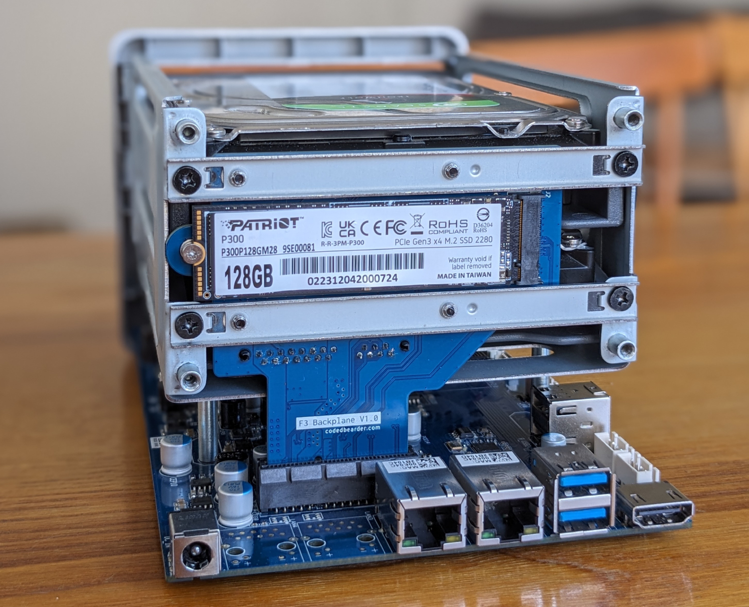
Blog post about creating this: https://codedbearder.com/posts/f3-backplane/
The gerber zip file can be found under fab/v1.0/f3_backplane.zip and is generated for JLCPCB. When ordering the PCB make sure to select impedance controlled stackup JLC04161H-7628.

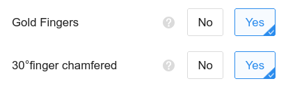
Also, make sure to select Gold Fingers and 30°finger chamfered. It will recommend selecting an ENIG surface finish in order to get them actually gold plated, but as this is more expensive and the backplane shouldn't get removed and inserted into the motherboard often I just went with the standard HASL (with lead) surface finish and I haven't had any problems.
| Qty | Value | Footprint | References |
|---|---|---|---|
| 15 | 100nF | Capacitor_SMD:C_0603_1608Metric | C6, C11, C14, C15, C17, C20, C21, C22, C31, C34, C35, C37, C40, C41, C42 |
| 8 | 22uF | Capacitor_SMD:C_0805_2012Metric | C12, C13, C18, C19, C32, C33, C38, C39 |
| 4 | 10uF | Capacitor_SMD:C_0805_2012Metric | C10, C16, C30, C36 |
| 4 | 2R2 | Resistor_SMD:R_2512_6332Metric | R1, R2, R3, R4 |
| 4 | MountingHole_Pad | Mounting:MountingHole_3.5mm_Pad_Via_With_Alignment_Hole | H1, H2, H3, H4 |
| 4 | NCP45521 | Load_Switches:NCP45521 | U1, U2, U3, U4 |
| 2 | 100n | Capacitor_SMD:C_0603_1608Metric | C4, C5 |
| 2 | 47u | Capacitor_SMD:C_0805_2012Metric | C1, C2 |
| 2 | SATA_Backplane | Connector_Backplane:Molex_0877011001 | J3, J4 |
| 1 | 22u | Capacitor_SMD:C_0805_2012Metric | C3 |
| 1 | Bus_M.2_Socket_M | Connector_Backplane:Amphenol_MDT420M01001 | J2 |
| 1 | LOGO | Logo:f3_logo | G*** |
| 1 | MMBT3904 | Package_TO_SOT_SMD:SOT-23 | Q1 |
| 1 | PCIEx4_HOST | Connector_Backplane:PCIEx4_HOST | J1 |
It measures 95.8 × 82.4 mm and has 4 copper layers, 1.61 mm thick.
50 parts, built around the MMBT3904. The full list of its parts is on this page, with links to each part's symbol and footprint where PCBKit's library has them.
From the arnarg/f3_backplane repository on GitHub, at the commit this page was made from: the board is f3_backplane.kicad_pcb and its schematic connector.kicad_sch. PCBKit opens the board in the browser, with nothing to install.
Its repository states no licence, so its author keeps all rights: ask arnarg before reusing the design.
TalismanDesign/PocketMage_PDA
An E-Ink PDA device using the ESP32 S3.

fossasia/pslab-hardware
PSLab Hardware Design and Schematics https://pslab.io


iMike78/nest-mini-drop-in-pcb
Drop-in PCB replacement for the Google Nest Mini v2 with ESP32-S3, ESP32-P4 and optional ESP32-C6. Inspired by Onju Voice and Home Assistant Voice PE.

ohmtech-rdi/eurorack-blocks
Software to Hardware Prototyping for Eurorack using C++, Max/Gen~ or Faust

Bellafaire/ESP32-Smart-Watch
An open source smartwatch based on the ESP32 compatible with the Arduino IDE.

AndersBNielsen/Relatively-Universal-ROM-Programmer
Hardware to program W27C512 EEPROM or any 24/28/32 pin ROM requiring from 5V to 27V programming voltage.