
2 layers
Nrf bga
github-linguist/linguist
Language Savant. If your repository's language is being reported incorrectly, send us a pull request!
12 parts14kMIT

A 6-key (3×2) macropad with a rotary encoder: 3D-printed case, custom 2-layer PCB, and KMK firmware, driven by a Seeed XIAO RP2040. Keys wire direct to GPIO (no matrix, no diodes), and the encoder handles volume/scroll.
Hexpad is an open-source printed circuit board by Antoncarlens-code, from the Antoncarlens-code/Hexpad-macropad repository on GitHub. It is a 2-layer board of 76 × 74 mm with 12 parts on 10 nets, routed with 58 tracks and 0 vias.
Its parts include 6 switches and 1 IC. It belongs with the RP2040 boards of this library.
A 6-key (3×2) macropad with a rotary encoder: 3D-printed case, custom 2-layer PCB, and KMK firmware, driven by a Seeed XIAO RP2040. Keys wire direct to GPIO (no matrix, no diodes), and the encoder handles volume/scroll.
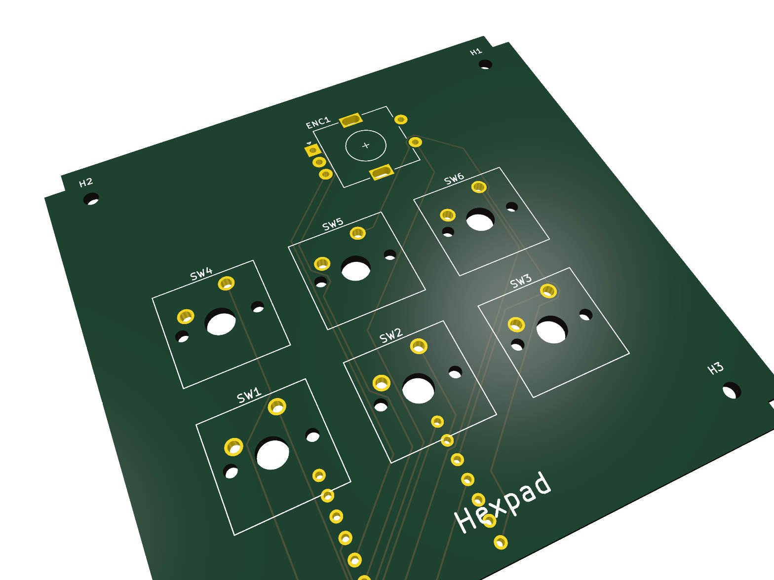
I wanted a compact editing/clipboard pad with a volume knob that didn't look like every other square macropad — so Hexpad uses a hexagonal silhouette around a centered 3×2 key cluster with the encoder up top.
Two things were genuinely fiddly. First, the original top-plate CAD came out of an
early IDE session malformed — the plate solid was fused to a stray slab 74 mm
below it, so it "levitated" in the slicer. I had to reverse-engineer the real
dimensions from the STEP geometry and rebuild the plate as a clean parametric
build123d script. Second, rather than hand-draw the board I generated the PCB
programmatically with KiCad's pcbnew API from a single coordinate spec, which
guarantees the switch, encoder, and mounting-hole positions line up exactly with
the printed plate (19.05 mm pitch, mounts at ±32 × ±31 mm).
| Schematic | PCB | Case |
|---|---|---|
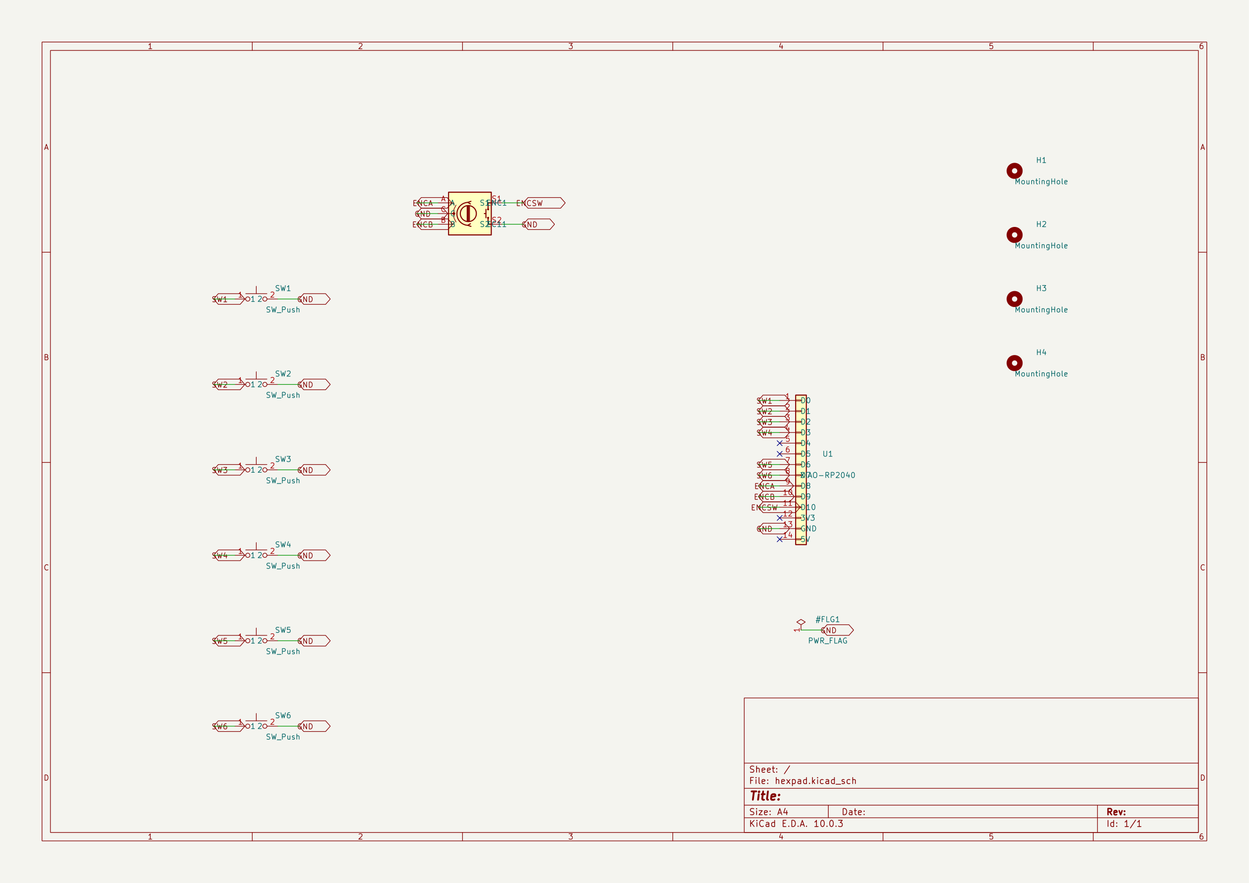 | 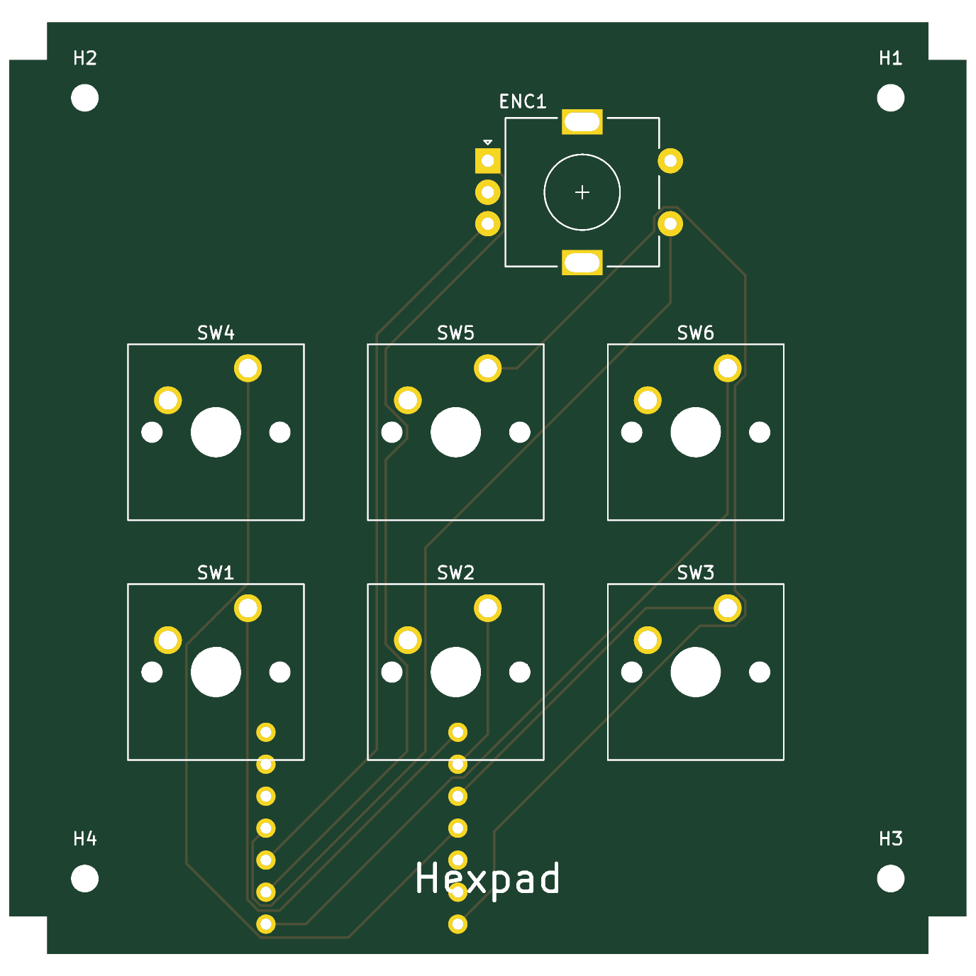 | 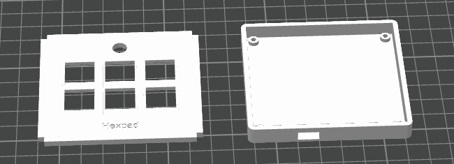 |
Full sheet: docs/electronics/hexpad-bom.csv.
| Qty | Part | Notes |
|---|---|---|
| 1 | Seeed XIAO RP2040 | MCU, mounted on the back; USB-C exits the front edge |
| 6 | Cherry MX (or compatible) switch | MX_Only_1.00u, direct-wired, one GPIO each |
| 1 | Alps EC11 rotary encoder w/ switch | A/B + push → 3 GPIO, common → GND |
| 4 | M2 screw (~6 mm) | through the case into the plate's corner posts |
| 6 / 1 | MX keycaps / encoder knob | cosmetic |
| 0 | diodes | none — direct wiring is valid for ≤7 keys |
| Folder | Contents |
|---|---|
cad/ | Enclosure: STEP blueprints + parametric build123d source |
pcb/ | KiCad 10 PCB project, schematic, + fabrication Gerbers |
firmware/ | KMK (CircuitPython) keymap |
docs/electronics/ | Schematic (SVG), BOM, PCB design notes |
docs/images/ | Render + schematic/PCB/case photos for this README |
| File | Purpose |
|---|---|
pcb/hexpad.kicad_sch | Schematic (XIAO + 6 switches + encoder) |
pcb/hexpad.kicad_pcb | KiCad 10 board, branded, routed |
pcb/hexpad-gerbers.zip | Upload to JLCPCB to order boards |
pcb/build_hexpad_pcb.py / build_hexpad_sch.py | Regenerate board/schematic from the spec |
2-layer, 76 × 74 mm (within the 100 mm limit), silkscreen-branded "Hexpad", matching the plate's switch / encoder / mounting coordinates.
KMK keymap at firmware/code.py. Default: front row Copy/Paste/Cut, rear row
Undo/Redo/Save, encoder = volume (press = mute). See firmware/README.md for
flashing and remapping.
| Input | XIAO pin | Input | XIAO pin | |
|---|---|---|---|---|
| SW1–SW3 (front) | D0, D1, D2 | Encoder A / B | D8 / D9 | |
| SW4–SW6 (rear) | D3, D6, D7 | Encoder push | D10 |
D4/D5 (SDA/SCL) left free for a future OLED. All inputs use the RP2040's
internal pull-ups.
build123d (CAD → STEP) · KiCad 10 (PCB) · Bambu Studio (slicing) · CircuitPython + KMK.
docs/images/)| Qty | Value | Footprint | References |
|---|---|---|---|
| 6 | SW_MX | SW_Cherry_MX_1.00u_PCB | SW1, SW2, SW3, SW4, SW5, SW6 |
| 4 | M2 | MountingHole_2.2mm_M2 | H1, H2, H3, H4 |
| 1 | EC11 | RotaryEncoder_Alps_EC11E-Switch_Vertical_H20mm | ENC1 |
| 1 | XIAO-RP2040 | U1 |
It measures 76 × 74 mm and has 2 copper layers, 1.6 mm thick.
12 parts. The full list of its parts is on this page, with links to each part's symbol and footprint where PCBKit's library has them.
From the Antoncarlens-code/Hexpad-macropad repository on GitHub, at the commit this page was made from: the board is pcb/hexpad.kicad_pcb and its schematic pcb/hexpad.kicad_sch. PCBKit opens the board in the browser, with nothing to install.
Its repository states no licence, so its author keeps all rights: ask Antoncarlens-code before reusing the design.
github-linguist/linguist
Language Savant. If your repository's language is being reported incorrectly, send us a pull request!


google/mozc-devices
Circuit diagrams and firmware source code for Gboard DIY keyboards


hackclub/OnBoard
💡 Join 1,000 teenagers and make your first PCB with a $100 grant!

VoronDesign/Voron-Tap
Tap is a nozzle-based z-probe for the V2 and Trident printer designs. The entire toolhead moves to trigger an optical switch. Tap offers many advantages:

stacksmashing/pico-tpmsniffer
A simple, very experimental TPM sniffer for LPC bus