
2 layers126 × 82 mm
Jackless Panel
AnotherBuildCorner/Relay_Switcher
DIY Relay bypass switcher for audio applications
298 parts

 AnotherBuildCorner/Relay_Switcher
DIY Relay bypass switcher for audio applications
V2 Loop Panel is an open-source printed circuit board by AnotherBuildCorner, from the AnotherBuildCorner/Relay_Switcher repository on GitHub. It is a 2-layer board of 112.3 × 87 mm with 180 parts on 96 nets, routed with 536 tracks and 4 vias.
It is built around the L7805. Its parts include 12 connectors, 8 resistors, 4 ICs and 4 diodes.
DIY Relay bypass switcher for audio applications
Are you a Guitarist/Bassist? Do you have a pedalboard that just keeps on getting more complicated?
Worried about losing the high end to the long capactive runs and buffers?
Or maybe you want the ability to control your Star-Trek level board from a small controller on your desk?
Or maybe you looked at the avaliable products, and practically fell out of your chair with the price tag?
Then look no further! In this project you'll find a modular capable, mono or stereo loop bypass switcher with wireless control capability.
V3 Jackless Is up and running in the same 6 back stacked form factor as V2. At this point I believe this represents the final version for this current system based on the WROOM32E. Why?
V2 Jackless is up and running in a 6 bay stacked model. In the process a handful of lessons were picked up.
The V3 Design implements some of the noted design problems from V2. Development has continued exclusively with the 3.5mm pitch model. As these are the parts I have on hand. and increasing the terminal block size appears to have little practical benefit.
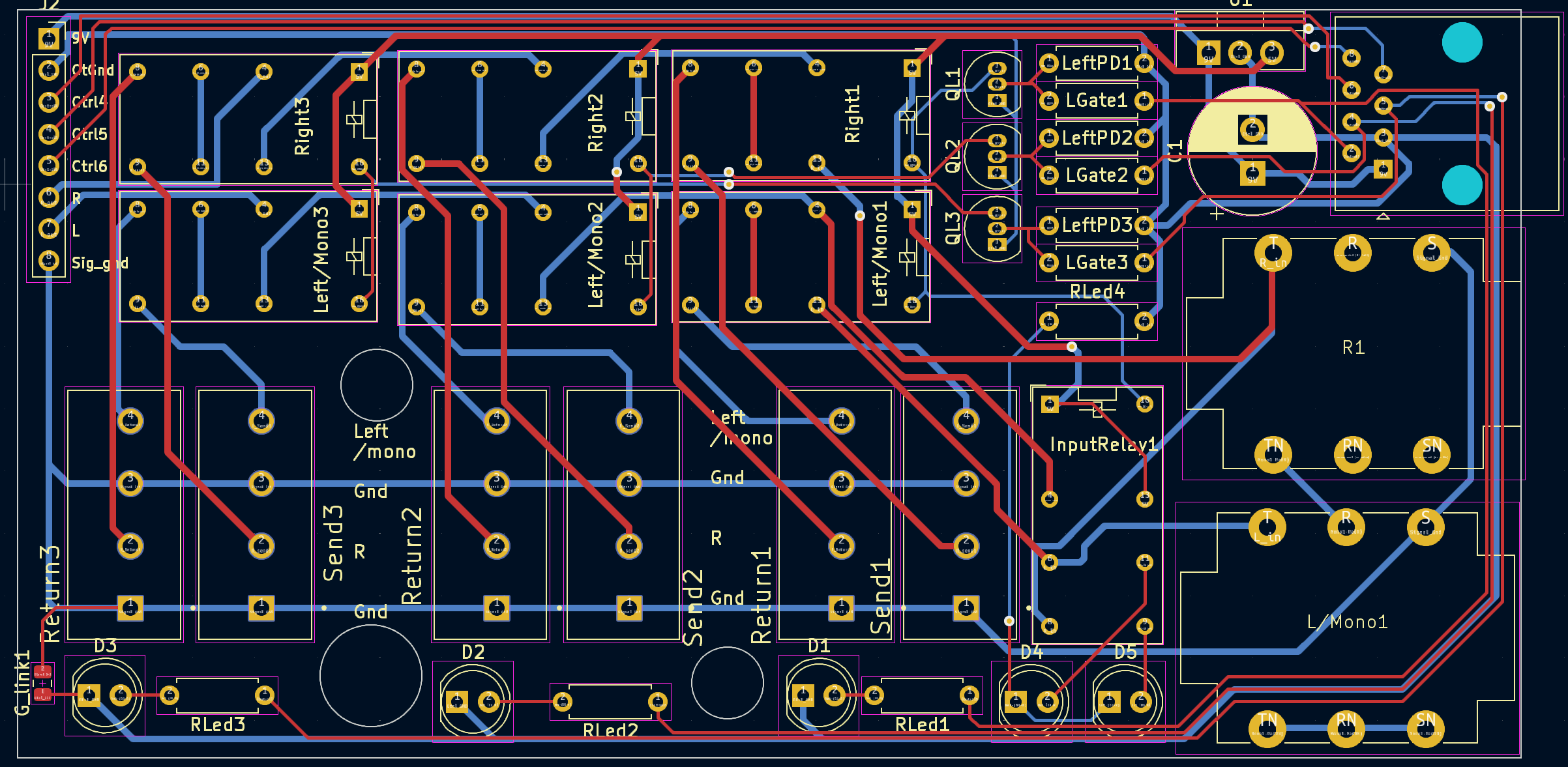
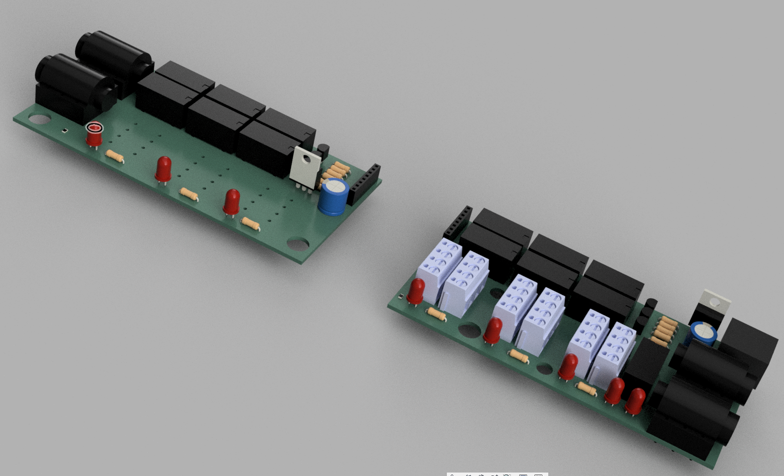
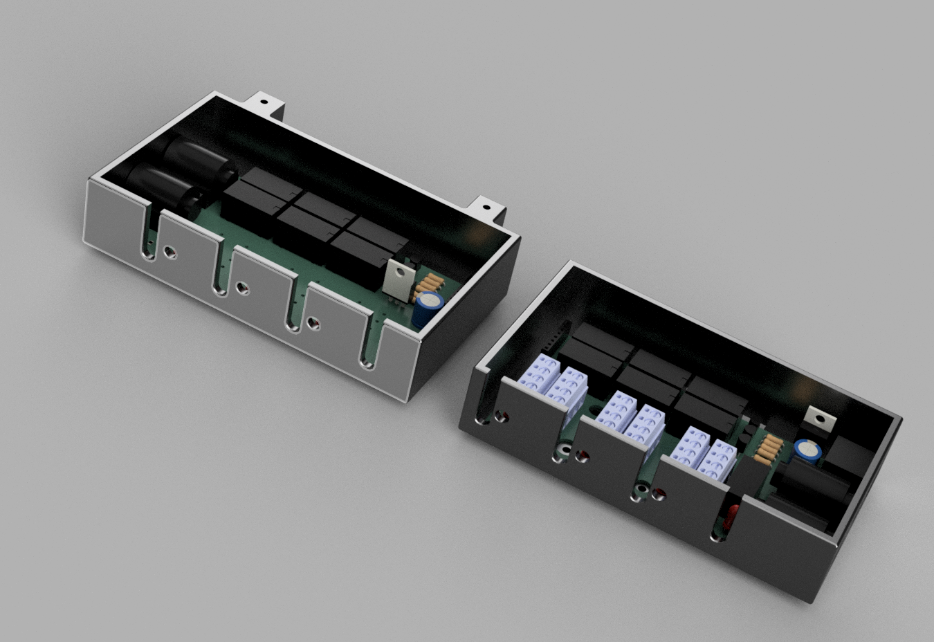
Instead of utilizing individual loop boards, there are now a pair of boards linked by a ribbon cable. As a set, these combined boards can support either 6 mono/stereo loops, or 5 mono/stero loops and a mono input selector depending on relay configuration.
Input Board
Output Board
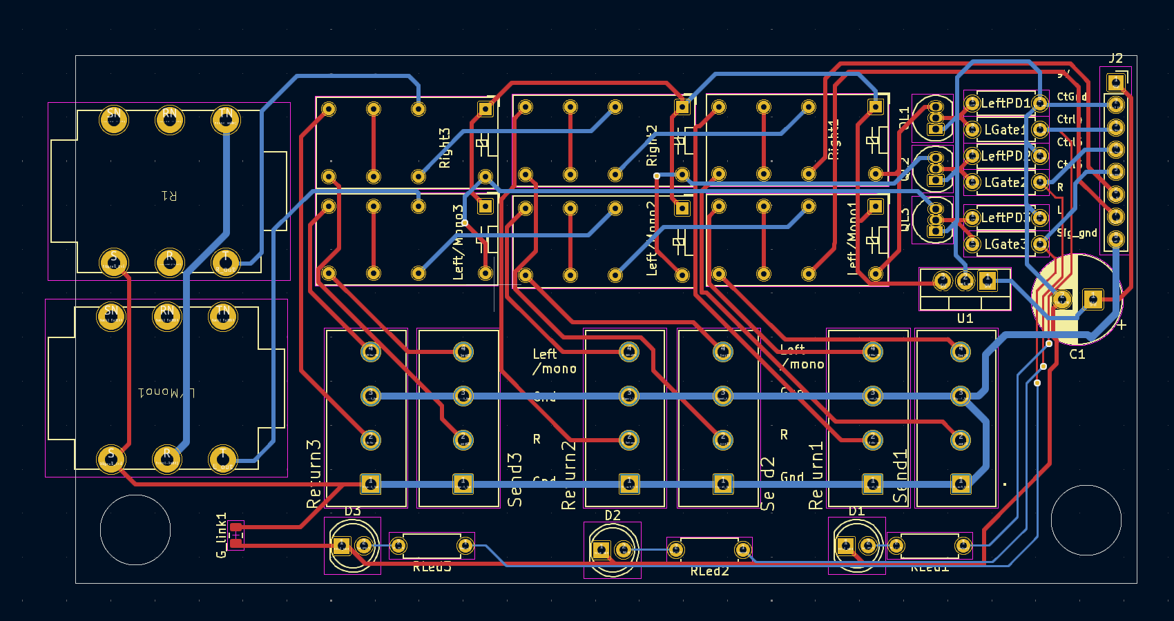
This change produces a couple of benefits. First is wiring is vastly improved. with the total wire soldering point count down from 7 per board ( L/R in, L/R out, Ground 9V, and Control signal.) Times 6 loop packages, for a total of 42 solder points. To 16 solder points total for the entire package. As well as being inline, ideal for a ribbon cable, as opposed to scattered across the board.
Additionally, the number of Voltage regulators is down from one per package, to one per PCB (with 3 loops on each). so a 66% reduction overall.
The mentioned power and signal ground linking has been added, provided by the G_link pads located on each PCB, in practice using booth may create a ground loop, so ideally soldering just one is reccomended.
Now the one loss from such a design (albeit minimal in practical usage) is the loops can no longer be order changed by moving around connectors inside the package (or perhaps in the future a complex multi relay network). In practice this just means physically changing the order of the connected devices at the device instead, and is a minimal downside.
Both Boards Populated
Complete Stacked model Assembly
V2 makes some significant improvements over the V1 design. And introduces a second design. the changes are as follows
Length of board reduced to 61mm Long
Reduced count of 2n7000 MOSFET drivers from 3 to 1
Tied status LED directly to the control output for a net -1 2n7000
Tied the two relay coils together, controlled by single 2n7000
Among the boards are now the standard stereo jack model, and a pair of new "jackless" models
The jackless models utilize either a 4x3.5mm pitch or 4x5mm pitch screw terminal block on the IO. this reduces the cost per loop by up $10 in full implementation
Additionally, it appears the space consumption overall will be significantly reduced with the new design
The reduced board size should enable either the w/ jack or jackless versions to fit inside a standard 1032L Aluminium looper case In testing, the relay coils consume 30mA each, well under the 2n7000's maximum 200mA current. the new status LED position can also function as a pulldown for the inputs, reduces the 2n7000 count. And the originals had some current leakage which caused the led to be partially illuminated all the time
Pictured above is the main relay board. The core Arcitecture is one 5V coil DPDT Relay per signal channel. So for stereo configurations, two relays are required. Each Relay is driven by a MOSFET 2n7000 switch circuit. As well as the status LED. All three MOSFET gates are tied to a common signal pin, and configured for 3.3V logic.
Each board is also equipped with a 74L05 5V regulator to drop the incoming 9V power, and provide supply for the relay switching.
Each board also has dual power connectors, as well as 3 pin 2.54mm spaced pins for the signal this alows for easy connections between multiple boards in series.
Finally, the boards are set up to accept switched 1/4 inch stereo jacks. With the switches internally connected, so loops without connections pass signal in either active or inactive state.
(Add PCB wire photos here)
Of further note, was the consideration to keep audio, and control/ power wires as far away, and with minimal crossing as possible. This is to reduce crosstalk from the processor and power supplies into the audio path.
Future iterations will focus on compressing the PCB into a space suitable for a 16L Aluminium looper enclosure. Or possibly a design set up to directly connect to the mono/stereo signal wires, therby reducing the need for the 1/4 Barrel connectors, and reducing the required 1/4 Plugs by 1/2. This also helps with space considerations. Considering these plugs cost upwards of $4 each, cutting in half is most welcome, although this reduces how universal this device will be.
Changes from V1 to V2 are a different footprint ESP32. now the Wroom 32E is the standard, with 38 pins avaiable.
The individual pin headers have been replaced by 3x rj45 connectors. each is configured with 6 individual GPIO pins, as well as a 9V connection, and ground.
Additionally, a new breakout board for the rj45 on the receiver end has been created.
The microprocessor controlling the relays is an ESP32 Devkit C V3 Chosen for it's relative availability, low price, access to Arduino IDE code, and most importantly the dedicated ESP_NOW wireless communication protocol, which will be used to communicate between boards. This is a relatively simple IO board for connecting to the GPIO of the processor board. The only extra element is another 74L05 voltage regulator connected to the 5V input of the dev board and the 4 pullup resistors slotted in on GPIO pins which only provide input (not suitable for the relay control, but there are already plenty of pins available for most applications).
One shortcoming, there may not be enough GPIO pins to handle the control switches, status LED's, screen, and rotary encoder(s). But this is all currently under development.
This version has a single easily remedied flaw. I had to create a footprint for the ESP32 used as they were what I had to hand, but appear to no longer be made. Well I flipped a ground and power connection, shorting 3.3V power to ground. For now it's just a matter of cutting the trace.
Future versions will probably switch to using a V4 devkit, or the newer devkits based on the S3 processor for more GPIO, and to retain more current availability.
The new V2 board corrects an error in the input switching, resulting in one of the inputs being completely unusable. Additionally, the board size has been significantly reduced in length. and the IO board direct pinouts have been moved directly under each jack.
This is very similar to the main relay boards. The differences are the use of the single relay, the dual LED indicators, and the large electrolytic capacitor on the 9V rail. The Capacitor is a filtering cap, as most of the 9V power supplies will be switched mode supplies, and noise prone. The relay is no longer used to enable/disable a loop. but instead is used to switch between two possible inputs/outputs. With the other half of the relay dedicated to controlling the indicator LED's lastly there are direct pinouts on the back of each 1/4 Barrel connector. Should switching features not be desired, these can be used to link the relay loops directly to an output without extra parts.
JAckless model.
The latest relay switch is setup to accept 5 of the jackless relay boards, and one V2 IO board with the RJ45 connection board in front. however this new model is half the height of V1, and is stackable. By splitting the units into modules of 5, this enables break points for things such as Volume pedals, and always on boosts between loop modules. Additional smaller size stackable modules will likely be produced in the future. No one single module can exceed more than 6 relay modules due to the RJ45 connection's configuration.
(picure) The current housing design uses horizontally stacked relay loops, with a total count of 10. Plus the input and output boards. The IO is located on the front for accesibility, with the loops located on the back.
(picture The current design is a single print, 6 switch control with provisions to add a 128X64 OLED. At present this is in it's early stages, so no provisions to mount the control board, or a larger screen have been included. This will come around in V2 The footswitches are spaced to allow foot, or hand use currently. And the board can be purely powered from a 5V usb supply though the ESP32 board.
(Coming Soon...)
| Qty | Value | Footprint | References |
|---|---|---|---|
| 112 | NPTH | NPTH | KiKit_MB_10_1, KiKit_MB_10_2, KiKit_MB_10_3, KiKit_MB_10_4, KiKit_MB_11_1, KiKit_MB_11_2, KiKit_MB_11_3, KiKit_MB_11_4, KiKit_MB_12_1, KiKit_MB_12_2, KiKit_MB_12_3, KiKit_MB_12_4, KiKit_MB_13_1, KiKit_MB_13_2, KiKit_MB_13_3, KiKit_MB_13_4 +96 |
| 8 | AudioJack3_Switch | Connector_Audio:Jack_6.35mm_Neutrik_NMJ6HFD3_Horizontal | Return1, Return1, Return1, Return1, Send1, Send1, Send1, Send1 |
| 8 | Conn_01x02_Pin | Connector_PinHeader_2.54mm:PinHeader_2x01_P2.54mm_Vertical | J2, J2, J2, J2, J3, J3, J3, J3 |
| 8 | Conn_01x03_Pin | Connector_PinHeader_2.54mm:PinHeader_1x03_P2.54mm_Vertical | In1, In1, In1, In1, Out1, Out1, Out1, Out1 |
| 8 | G5V-2 | Relay_THT:Relay_DPDT_Omron_G5V-2 | Left/Mono1, Left/Mono1, Left/Mono1, Left/Mono1, Right1, Right1, Right1, Right1 |
| 8 | R | Resistor_SMD:R_0201_0603Metric | R8, R8, R8, R8, R9, R9, R9, R9 |
| 8 | R | Resistor_THT:R_Axial_DIN0207_L6.3mm_D2.5mm_P7.62mm_Horizontal | LeftPD1, LeftPD1, LeftPD1, LeftPD1, LGate1, LGate1, LGate1, LGate1 |
| 4 | 100 | Resistor_THT:R_Axial_DIN0207_L6.3mm_D2.5mm_P7.62mm_Horizontal | RLed1, RLed1, RLed1, RLed1 |
| 4 | 2N7000 | Package_TO_SOT_THT:TO-92_Inline | QL1, QL1, QL1, QL1 |
| 4 | Conn_01x01_Pin | Connector_PinHeader_2.54mm:PinHeader_1x01_P2.54mm_Vertical | J1, J1, J1, J1 |
| 4 | L7805 | Package_TO_SOT_THT:TO-220-3_Vertical | U1, U1, U1, U1 |
| 4 | LED | LED_THT:LED_D5.0mm | D1, D1, D1, D1 |
It measures 112.3 × 87 mm and has 2 copper layers, 1.6 mm thick.
180 parts, built around the L7805. The full list of its parts is on this page, with links to each part's symbol and footprint where PCBKit's library has them.
From the AnotherBuildCorner/Relay_Switcher repository on GitHub, at the commit this page was made from: the board is PCB's/Loop Board V2/V2 Loop Panel/V2 Loop Panel.kicad_pcb. PCBKit opens the board in the browser, with nothing to install.
Its repository states no licence, so its author keeps all rights: ask AnotherBuildCorner before reusing the design.
AnotherBuildCorner/Relay_Switcher
DIY Relay bypass switcher for audio applications

AnotherBuildCorner/Relay_Switcher
DIY Relay bypass switcher for audio applications

AnotherBuildCorner/Relay_Switcher
DIY Relay bypass switcher for audio applications

AnotherBuildCorner/Relay_Switcher
DIY Relay bypass switcher for audio applications


AnotherBuildCorner/Relay_Switcher
DIY Relay bypass switcher for audio applications

AnotherBuildCorner/Relay_Switcher
DIY Relay bypass switcher for audio applications

AnotherBuildCorner/Relay_Switcher
DIY Relay bypass switcher for audio applications

AnotherBuildCorner/Relay_Switcher
DIY Relay bypass switcher for audio applications

AnotherBuildCorner/Relay_Switcher
DIY Relay bypass switcher for audio applications

AnotherBuildCorner/Relay_Switcher
DIY Relay bypass switcher for audio applications

AnotherBuildCorner/Relay_Switcher
DIY Relay bypass switcher for audio applications

Allen-Synthesis/EuroPi
EuroPi: A reprogrammable Eurorack module based on the Raspberry Pi Pico

peterheinrich/InternetOverSpaghetti
Transmitting IP packages over a pair of spaghetti thus demonstrating how media independent IP really is.


Tircown/ERCF-easy-brd
More informations on how to reset for flashing:\ https://wiki.seeedstudio.com/Seeeduino-XIAO/#enter-bootloader-mode

matthewcieplak/super-sixteen
Code and schematics for the Super Sixteen Eurorack sequencer

NikodemBartnik/Mini-Mars-Rover
Educational robotic platform made to look like a mini mars rover

starlightk7/OpenSFC
OSHW Reproduction Parts related to the Super Famicom / Super Nintendo game console

Redherring32/OpenTendo-TopLoader
An Open Source HardWare (OSHW) recreation of the 1993 toploading NES motherboard (Also known as NES-101)