
4 layers150 × 150 mm
DigitalOsciloscope
PiatekBartosz/DigitalOscilloscope_Hardware
Hardware for digital oscilloscope project
387 parts1

 anikjain11/OpenDAQ-MixedSignal-AFE1
It takes a sub-nanosecond, femtocoulomb-level current pulse generated by a particle hit on a semiconductor sensor, processes it through an ultra-low noise analog front-end (AFE), and digitizes the signal via a…
Opa656 test is an open-source printed circuit board by anikjain11, from the anikjain11/OpenDAQ-MixedSignal-AFE repository on GitHub. It is a 4-layer board of 67 × 17 mm with 18 parts on 13 nets, routed with 120 tracks and 12 vias.
It is built around the OPA656U. Its parts include 3 crystals, 2 resistors and 1 connector.



 [blocked]
OpenDAQ-AFE is an open-source, production-grade mixed-signal data acquisition (DAQ) and detector front-end architecture. Designed for high-energy physics instrumentation, this system bridges microscopic sensor physics to real-time digital signal processing.
It takes a sub-nanosecond, femtocoulomb-level current pulse generated by a particle hit on a semiconductor sensor, processes it through an ultra-low noise analog front-end (AFE), and digitizes the signal via a high-speed path.
[ Semiconductor Sensor (PIN Diode / 70pF) ]
                       │
                       ▼ (1 pC Charge Pulse, ~1ns rise)
[ Analog Front-End (OPA656 Charge-Sensitive Preamplifier) ]
                       │
                       ▼ (-900mV Step, 50us Exponential Decay)
[ Active CR-RC Pulse Shaper with PZ Cancellation ]
                       │
                       ▼ (~720mV Semi-Gaussian shaping peak)
[ High-Speed Flash ADC & FPGA RTL Engine ]
                       │
                       ▼ (Digitized Event Frames)
[ CERN ROOT / Python Analysis Pipeline ]OpenDAQ-MixedSignal-AFE/
├── hardware_kicad/ # 4-Layer PCB schematics, layout (.kicad_pcb), and Gerbers
├── simulations_spice/ # Ngspice netlists, subcircuits (.sub), and transient analysis
│ └── CSP_FrontEnd_Simulation/
│ ├── opa656.sub
│ └── README.md # Detailed SPICE math and slew-rate bottleneck logs
├── results/ # Visual proof and exported documentation
│ ├── 01_simulations/ # Python-plotted transient response graphs
│ ├── 02_schematics/ # PDF exports of system architecture
│ └── 03_pcb_layout/ # 2D routing and 3D board renders
└── README.md # Main project overview (You are here)The Charge-Sensitive Preamplifier (CSP) converts input charge ($Q_{in}$) into a proportional voltage step via feedback capacitance ($C_f = 1\text{ pF}$). To prevent pulse pile-up at high event rates, the 50µs CSP decay tail is compressed using an active shaping amplifier. A Pole-Zero (PZ) cancellation network perfectly counteracts the CSP's discharge time constant.
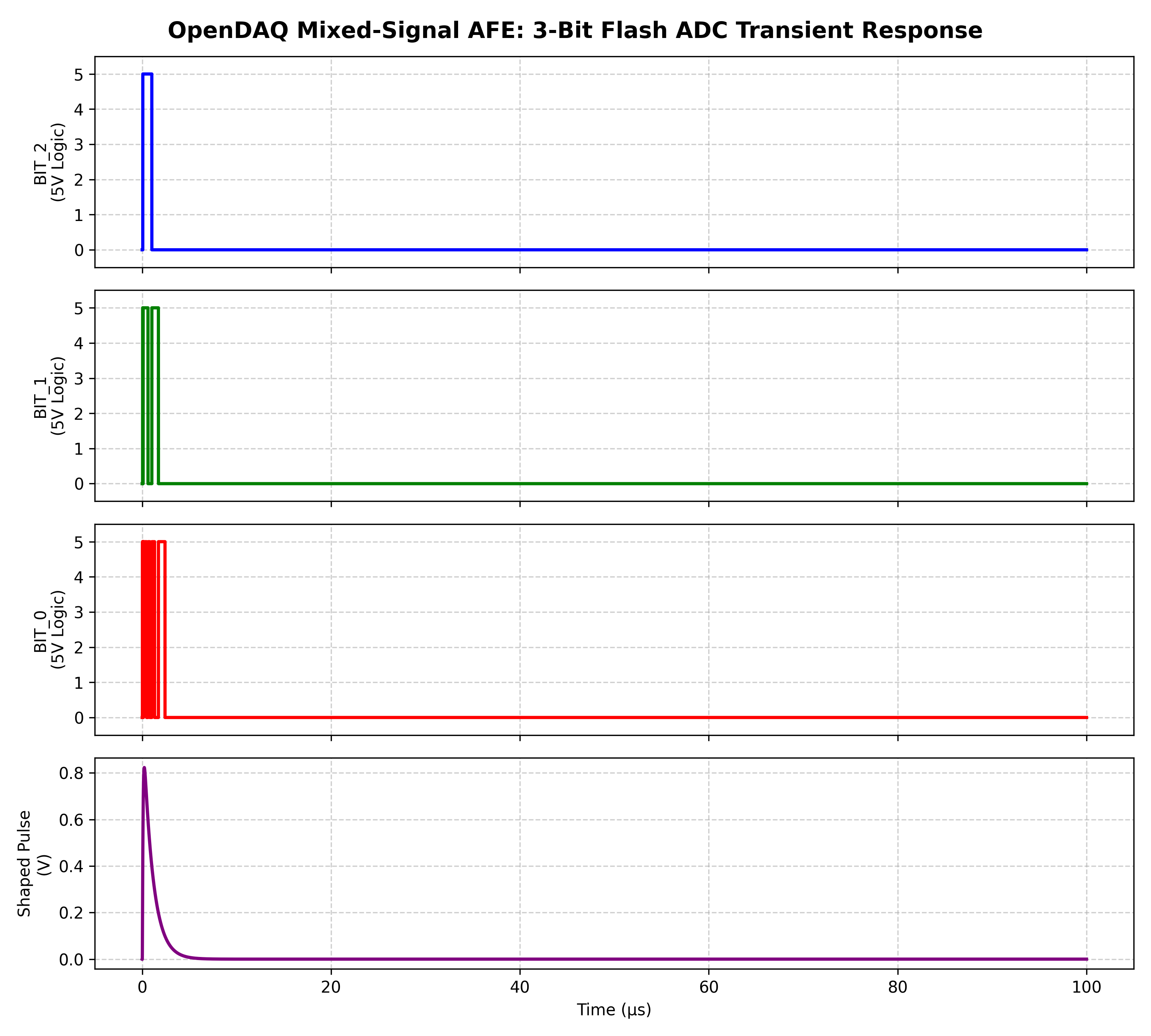
Above: Ngspice transient analysis displaying the shaper compressing the 50µs tail into a clean ~720mV semi-Gaussian peak, triggering the 3-bit Flash ADC logic (111). Note: For a deep dive into the SPICE slew-rate limitations and behavioral modeling of the ADC, read the Simulation Notes here.
To translate the physics into silicon, the AFE was routed onto a strictly constrained, tapeout-ready physical board.
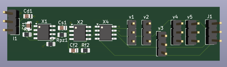
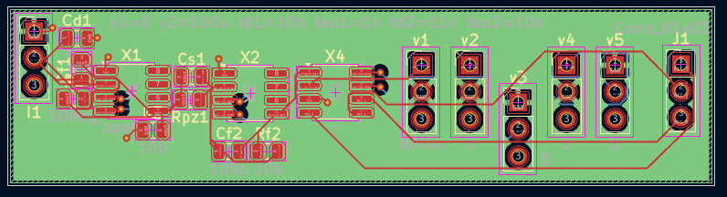
This hardware design and its associated software simulations are licensed under the CERN Open Hardware Licence v2.0 - Strongly Reciprocal (CERN-OHL-S). See the LICENSE file for details.
| Qty | Value | Footprint | References |
|---|---|---|---|
| 4 | 5 | Connector_PinHeader_2.54mm:PinHeader_1x03_P2.54mm_Vertical | v2, v3, v4, v5 |
| 2 | 100p | Capacitor_SMD:C_0805_2012Metric | Cf2, Cs1 |
| 2 | opa656 | Package_SO:SOIC-8_3.9x4.9mm_P1.27mm | X1, X2 |
| 1 | 100 | Resistor_SMD:R_0805_2012Metric | R3 |
| 1 | 10k | Resistor_SMD:R_0805_2012Metric | Rf2 |
| 1 | 1p | Capacitor_SMD:C_0805_2012Metric | Cf1 |
| 1 | 500k | Resistor_SMD:R_0805_2012Metric | Rpz1 |
| 1 | 50Meg | Resistor_SMD:R_0805_2012Metric | R1 |
| 1 | 70p | Capacitor_SMD:C_0805_2012Metric | Cd1 |
| 1 | 800m | Connector_PinHeader_2.54mm:PinHeader_1x03_P2.54mm_Vertical | v1 |
| 1 | Conn_01x03 | Connector_PinHeader_2.54mm:PinHeader_1x03_P2.54mm_Vertical | J1 |
| 1 | y1=0 y2=100u td1=10n tau1=1n td2=11n tau2=10n | Connector_PinHeader_2.54mm:PinHeader_1x03_P2.54mm_Vertical | I1 |
| 1 | ~ | Package_SO:SOIC-8_3.9x4.9mm_P1.27mm | X4 |
PiatekBartosz/DigitalOscilloscope_Hardware
Hardware for digital oscilloscope project


nanographs/Open-Beam-Interface
Just what you need to control the beam and get an image.


khill25/Dreamdrive
Open source Retro Rom Carts and ODEs by Dreamcraft Industries

mirdej/vmix
Multichannel modular analog PAL video mixer based on the SYNKIE project
It measures 67 × 17 mm and has 4 copper layers, 1.6 mm thick.
18 parts, built around the OPA656U. The full list of its parts is on this page, with links to each part's symbol and footprint where PCBKit's library has them.
From the anikjain11/OpenDAQ-MixedSignal-AFE repository on GitHub, at the commit this page was made from: the board is simulations_spice/CSP_FrontEnd_Simulation/opa656_test.kicad_pcb and its schematic hardware_kicad/opa656_test.kicad_sch. PCBKit opens the board in the browser, with nothing to install.
Its repository states no licence, so its author keeps all rights: ask anikjain11 before reusing the design.