
2 layers59.1 × 82.5 mm
 androda/F4_BlueSCSI24
A small SCSI device based on STM32F4
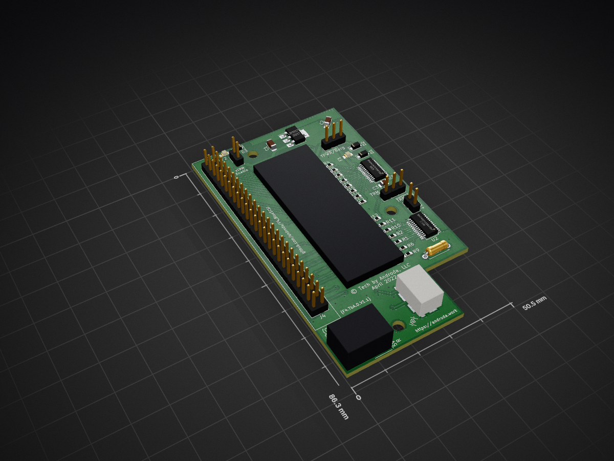
F4 SMD V1 1 is an open-source printed circuit board by androda, from the androda/F4_BlueSCSI repository on GitHub. It is a 2-layer board of 50.5 × 86.3 mm with 42 parts on 80 nets, routed with 770 tracks and 108 vias.
It is built around the LD1117V. Its parts include 19 resistors, 7 connectors, 3 capacitors, 3 ICs and 3 diodes.
| Qty | Value | Footprint | References |
|---|---|---|---|
| 18 | 110 ohm 1% | Resistor_SMD:R_0603_1608Metric_Pad1.05x0.95mm_HandSolder | R1, R2, R3, R4, R5, R6, R7, R10, R11, R12, R13, R14, R15, R16, R17, R18 +2 |
| 3 | Schottky Diode, 1A forward, 30V reverse | Diode_SMD:D_SOD-123F | D1, D2, D3 |
| 2 | 20uF | Capacitor_SMD:C_1206_3216Metric_Pad1.42x1.75mm_HandSolder | C1, C2 |
| 2 | 500mA Hold | Fuse:Fuse_0805_2012Metric_Castellated | F1, F2 |
| 2 | Conn_01x02_Male | Connector_PinHeader_2.54mm:PinHeader_1x02_P2.54mm_Vertical | J1, J3 |
| 2 | Conn_01x03_Male | Connector_PinHeader_2.54mm:PinHeader_1x03_P2.54mm_Vertical | J6, USBPWR |
| 2 | SN74CBTD3861DBQR | Package_SO:SSOP-24_3.9x8.7mm_P0.635mm | U2, U3 |
| 1 | 105162-0001 | CustomFootprints:microsd_molex_1051620001 | J5 |
| 1 | 4.7uF | Capacitor_SMD:C_0805_2012Metric_Pad1.15x1.40mm_HandSolder | C3 |
| 1 | 470 | Resistor_THT:R_Axial_DIN0207_L6.3mm_D2.5mm_P7.62mm_Horizontal | R19 |
| 1 | BergFloppy | CustomFootprints:BergFloppy_RightAngle | J2 |
| 1 | F4_Footprint | CustomFootprints:BluePillModule | BP1 |
| 1 | LD1117V | Package_TO_SOT_SMD:SOT-223-3_TabPin2 | U1 |
| 1 | SCSI_50Pin | CustomFootprints:SCSI_Internal_50Pin | J4 |
The 38 most common of 42 parts.


AbhiramV010/CarbonAwareCharge
The Carbon-Aware Charging logic & KiCad Schematics that were used in my STEAM ICAC 2026 Project. It will work for other applications as well.


1440pQHD/One-board-Air-quality-sensor
A simple, cheap-to-build PCB that actively monitors air quality and prevents invisible hazards. It makes protection from enviromental hazards accesible to everyone.


himanivishwa/S3DUCKY
A pocket-sized USB HID injection tool built on the ESP32-S3's native USB peripheral — no separate USB-serial or "Digispark"-style bootloader chip needed. Plug it in, and it enumerates as a keyboard.

mbouyer/canbus_transeiver_adapter
A breadboard-friendly CAN transeiver

rusefi/rusefi
rusefi - GPL internal combustion engine control unit
It measures 50.5 × 86.3 mm and has 2 copper layers, 1.6 mm thick.
42 parts, built around the LD1117V. The full list of its parts is on this page, with links to each part's symbol and footprint where PCBKit's library has them.
From the androda/F4_BlueSCSI repository on GitHub, at the commit this page was made from: the board is hw/Desktop_50Pin/F4_SMD_V1_1/F4_SMD_V1_1.kicad_pcb and its schematic hw/Desktop_50Pin/F4Lite_THTV1.1/F4Lite_THTV1_1.kicad_sch. PCBKit opens the board in the browser, with nothing to install.
Its repository states no licence, so its author keeps all rights: ask androda before reusing the design.