4 layers51.8 × 20 mm
Sample target
alvarop/swd2usbc
Have you ever wanted to debug your device over USB-C? Sometimes there's not enough room for a JTAG/SWD connector, or even Tag-Connect pads!
57 parts29CC0-1.0
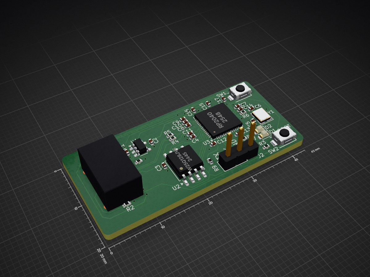
 alvarop/swd2usbc29
Have you ever wanted to debug your device over USB-C? Sometimes there's not enough room for a JTAG/SWD connector, or even Tag-Connect pads!
Sample target basic is an open-source printed circuit board by alvarop, from the alvarop/swd2usbc repository on GitHub, published under the CC0-1.0 licence. It is a 2-layer board of 43 × 20 mm with 46 parts on 65 nets, routed with 390 tracks and 47 vias.
It is built around the RP2040, W25Q128JVSIQ and MIC5504-3.3YM5-TR, with the CL05B104KB54PNC, SKRKAEE020 and ABM8-272-T3 among its other parts. Its parts include 17 capacitors, 9 resistors, 3 ICs, 2 diodes and 2 connectors. It belongs with the RP2040 boards of this library.


Have you ever wanted to debug your device over USB-C? Sometimes there's not enough room for a JTAG/SWD connector, or even Tag-Connect pads!
For history and all of the details, check out my detailed write up here.
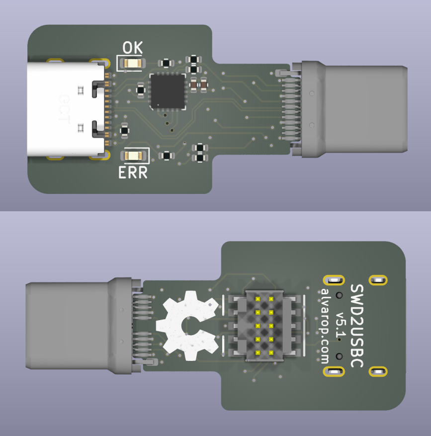
Full featured adapter with Debug Accessory Mode support. Includes an ATTiny microcontroller to set the correct pull-up resistors on CC1/CC2 to provide accurate charge current to the target. Has a USB-C plug so no extra USB-C cable required
The ATTiny firmware doesn't do much. It reads the voltage on the CC1/CC2 line that is pulled up and determines the available charge current. It then pulls up CC1 and CC2 to provide the charge current to the device under Debug Accessory Mode.
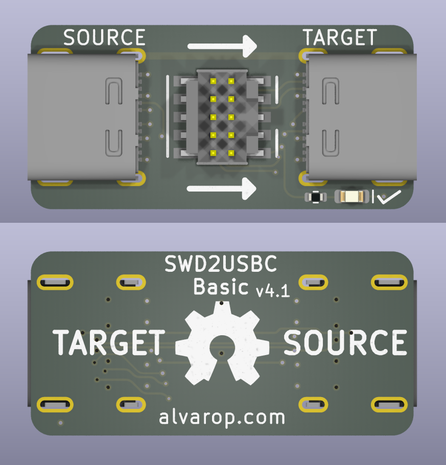 Simple adapter with no Debug Accessory Mode. Assumes target SWD lines wired up directly to TX1/2 as listed above. Requires USB3/Thunderbolt C to C cable to connect to target.
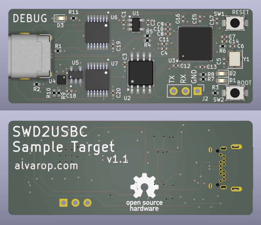
Example target device. Fully featured with CC1/2 comparators to connect/disconnect SWD lines if Debug Accessory Mode is active. Target is an RP2040 instead of STM32 since it's easier to source.
The sample target firmware does basic USB charge detection using the CC lines. When the Debug Accessory Mode is enabled, both CC1/CC2 are used, otherwise, the single CC line is used. There's an LED (D3) which lights up when Debug Accessory Mode is enabled.
The charge current is printed out over UART, but it is also displayed using the two LEDs. The blink patterns are:
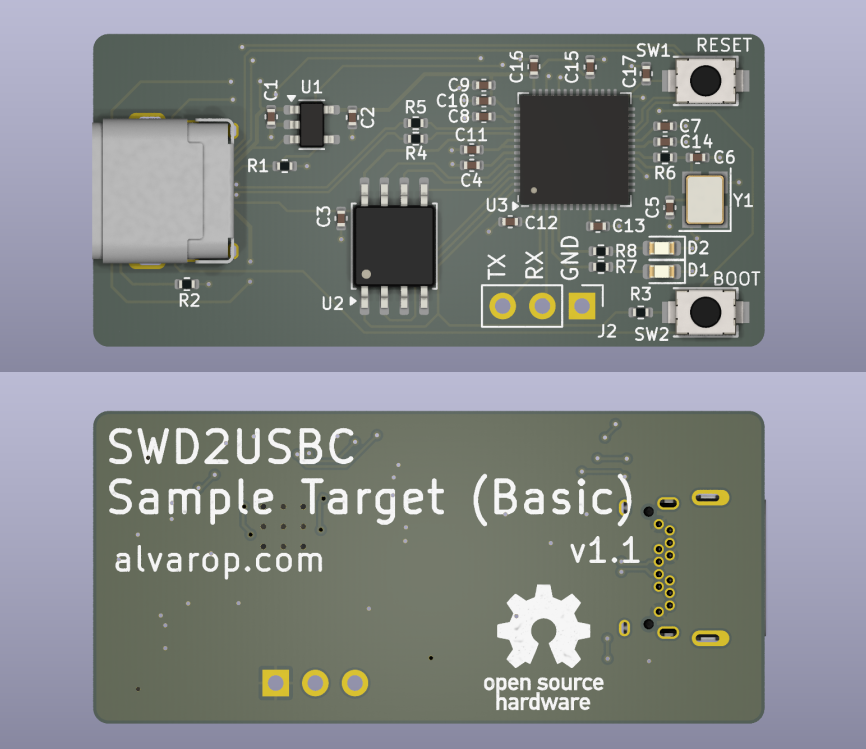
Basic example target. Similar to the sample target above, but does not include any comparators/switches. SWD lines are directly connected to the USB-C connector.
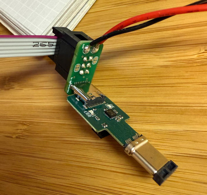
Simple adapter PCB to connect the AVRISP V2 connector to USB-C to program the ATTiny in the SWD2USBC device.
| Qty | Value | Footprint | References |
|---|---|---|---|
| 11 | 0.1uF | Capacitor_SMD:C_0402_1005Metric | C3, C4, C7, C9, C11, C12, C13, C14, C15, C16, C17 |
| 9 | , , , , , , , , | ||
| 4 | 1uF | Capacitor_SMD:C_0402_1005Metric | C1, C2, C8, C10 |
| 4 | 5.1k | Resistor_SMD:R_0402_1005Metric | R1, R2, R7, R8 |
| 3 | 1k | Resistor_SMD:R_0402_1005Metric | R3, R6, R9 |
| 2 | 15p | Capacitor_SMD:C_0402_1005Metric | C5, C6 |
| 2 | 27 | Resistor_SMD:R_0402_1005Metric | R4, R5 |
| 2 | LED | LED_SMD:LED_0603_1608Metric | D1, D2 |
| 2 | SW_Push | easyeda:SW-SMD_L3.9-W3.0-P4.45 | SW1, SW2 |
| 1 | ABM8-272-T3 | Crystal:Crystal_SMD_3225-4Pin_3.2x2.5mm | Y1 |
| 1 | Conn_01x03 | Connector_PinHeader_2.54mm:PinHeader_1x03_P2.54mm_Vertical | J2 |
| 1 | MIC5504-3.3YM5 | Package_TO_SOT_SMD:SOT-23-5 | U1 |
| 1 | RP2040 | Package_DFN_QFN:QFN-56-1EP_7x7mm_P0.4mm_EP3.2x3.2mm | U3 |
| 1 | USB_C_Receptacle | alvarop:UT11113-11602-7H | J1 |
| 1 | W25Q128JVS | Package_SO:SOIC-8_5.23x5.23mm_P1.27mm | U2 |
The 45 most common of 46 parts.
It measures 43 × 20 mm and has 2 copper layers, 1.6 mm thick.
46 parts, built around the RP2040, W25Q128JVSIQ, MIC5504-3.3YM5-TR and CL05B104KB54PNC. The full list of its parts is on this page, with links to each part's symbol and footprint where PCBKit's library has them.
From the alvarop/swd2usbc repository on GitHub, at the commit this page was made from: the board is sample-target-basic/sample-target-basic.kicad_pcb and its schematic sample-target-basic/sample-target-basic.kicad_sch. PCBKit opens the board in the browser, with nothing to install.
Its repository publishes it under the CC0-1.0 licence: you may reuse it on that licence's terms (keep the author's notice, and for a copyleft licence share your changes alike).
alvarop/swd2usbc
Have you ever wanted to debug your device over USB-C? Sometimes there's not enough room for a JTAG/SWD connector, or even Tag-Connect pads!

alvarop/swd2usbc
Have you ever wanted to debug your device over USB-C? Sometimes there's not enough room for a JTAG/SWD connector, or even Tag-Connect pads!

alvarop/swd2usbc
Have you ever wanted to debug your device over USB-C? Sometimes there's not enough room for a JTAG/SWD connector, or even Tag-Connect pads!

alvarop/swd2usbc
Have you ever wanted to debug your device over USB-C? Sometimes there's not enough room for a JTAG/SWD connector, or even Tag-Connect pads!


williamjroche/Drone_Flight_Controller
This is a GPS-Denied Autonomous Drone that uses computer vision to fly with radio transmission override. Autonomy is a work in progress.

ratmuds/spark
The PCB files for this project. The gerber and other PCBA files are in the production folder.

jackw01/scanlight
A better light source for scanning color negative film

alvarop/chaac
This is a work in progress for a wireless weather station project.


ikajdan/katia
A split keyboard with 6 by 3 column staggered keys and 3 thumb keys, based on the Crkbrd design