4 layers106 × 63.5 mm

 alexDickhans/self-cap
A small self-capacitance board from the HIRO Group. An ESP32-C6-MINI-1 reads seven electrode holes along one edge. Power comes from USB-C or a single-cell battery on a JST PH connector.
Self cap is an open-source printed circuit board by alexDickhans, from the alexDickhans/self-cap repository on GitHub. It is a 4-layer board of 45.2 × 19.8 mm with 29 parts on 41 nets, routed with 279 tracks and 39 vias.
It is built around the ESP32-C6-MINI-1, MAX40200AUK and SPX3819M5-L-3-3. Its parts include 12 resistors, 7 capacitors, 3 ICs, 3 connectors and 2 diodes. It belongs with the ESP32 and RISC-V boards of this library.


A small self-capacitance board from the HIRO Group. An ESP32-C6-MINI-1 reads seven electrode holes along one edge. Power comes from USB-C or a single-cell battery on a JST PH connector.
Open self-cap.kicad_pro in KiCad 9. The electrode-hole footprint lives in self-cap-conn.pretty. The silkscreen reads HIRO Group Self-Cap PCB v1.
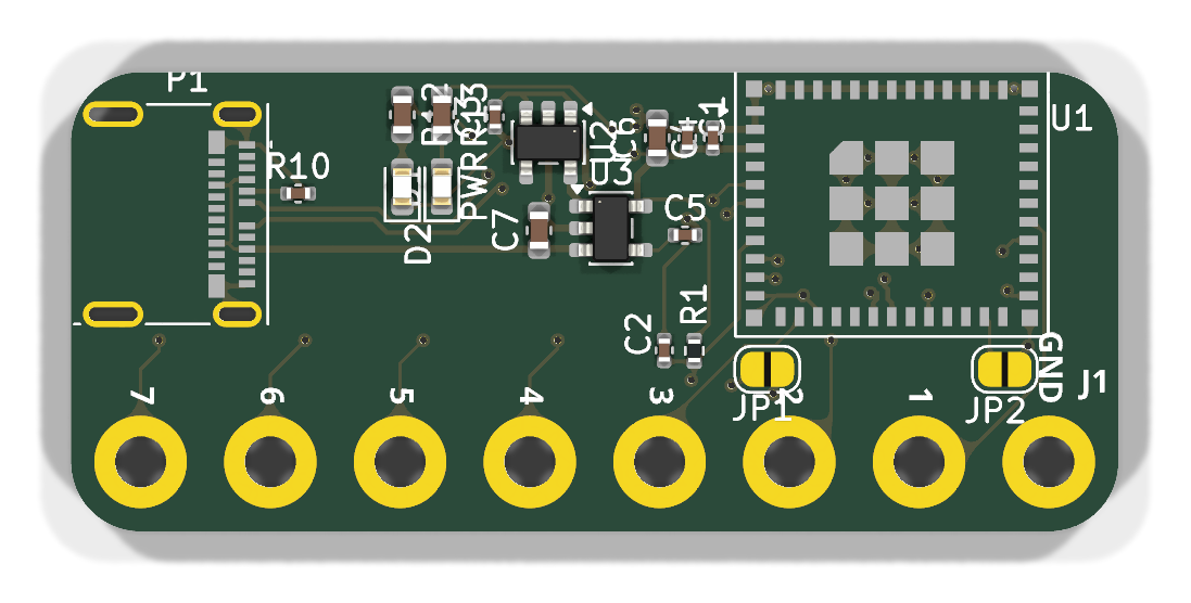
Top. The ESP32-C6-MINI-1 lands on the right, and the USB-C receptacle is the pair of slots on the left. The module can and the connector shell are not drawn here; the footprints are.
Bottom. J2 is the battery connector and R2 (1 kΩ) is fitted. R3–R9 are left empty.
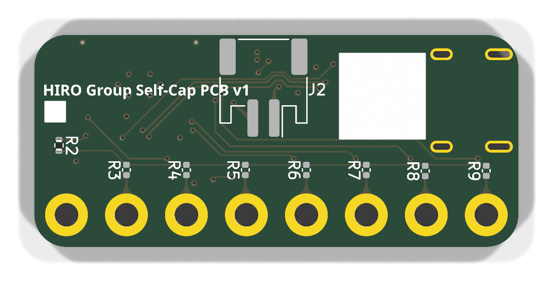
The board is 45.2 mm × 19.8 mm, four layers, 1.6 mm. The two inner layers are ground. Eight plated holes, 2.2 mm drill on a 5.6 mm pitch, run along the long edge. GND is the hole at the module end. Hole 7 is the hole at the USB end.
| Silkscreen | ESP32-C6 pin |
|---|---|
| GND | GND |
| 1 | IO23 |
| 2 | IO22 |
| 3 | IO1 |
| 4 | IO5 |
| 5 | IO4 |
| 6 | IO3 |
| 7 | IO2 |
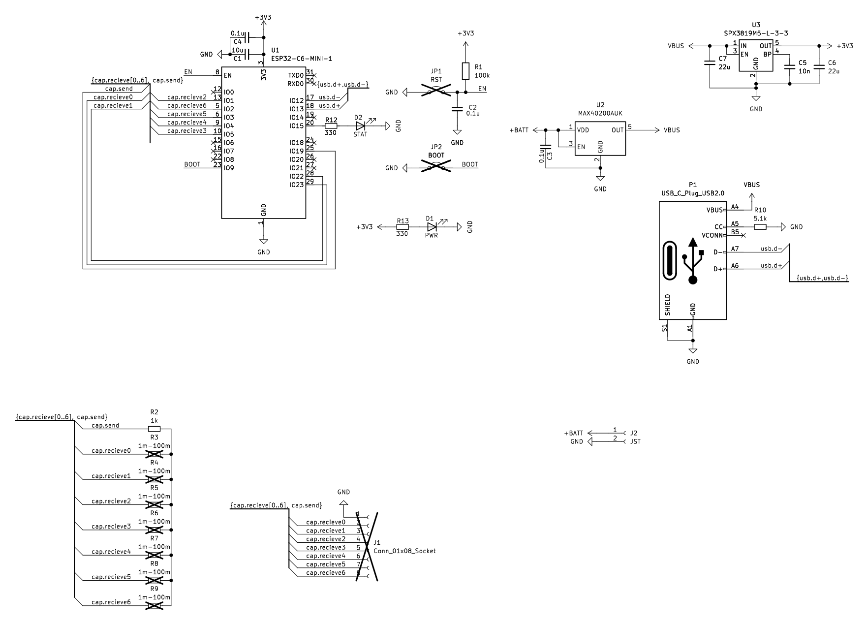
Each numbered hole is already tied to that GPIO. R3–R9 are optional 0402 resistors on the bottom, one per hole, from the electrode to a common node. That node is driven by IO19 through R2 (1 kΩ). The value on the schematic is 1 MΩ–100 MΩ; fit whatever value you want in that range, or leave them off.
D1 is the power LED. It lights when the 3.3 V rail is up. D2 is the status LED on IO15, active high, through 330 Ω.
JP1 and JP2 are open solder jumpers. Bridge JP1 to hold EN low. Bridge JP2 to hold IO9 (BOOT) low for the serial download mode. R1 is a 100 kΩ pull-up on EN.
USB-C or the battery can run the board. U3 (SPX3819) makes 3.3 V from that input. J2 pin 1 is battery positive and pin 2 is ground. Use a single lithium cell.
U2 (MAX40200) is an ideal diode from the battery onto the 5 V rail, so USB voltage stays off the cell. There is no charger on this board.
The USB 2.0 pair and the 5.1 kΩ CC pulldown are wired on one side of the receptacle (A6, A7, and A5). If a cable does nothing, flip the plug.
The files in production/ match this revision of the board. Upload those, not an older export.
production/self-cap-gerbers.zip. It contains the four copper layers, solder mask, silkscreen, paste, the board outline, and one Excellon drill file.| Setting | Value |
|---|---|
| Layers | 4 |
| Thickness | 1.6 mm |
| Material | FR-4 |
| Outer copper | 1 oz |
| Inner copper | 0.5 oz |
| Min trace / space | 0.15 mm / 0.2 mm |
| Smallest drill | 0.3 mm vias. Electrode holes are 2.2 mm. |
| Holes | All plated, including the electrode holes. The USB shell uses plated slots. |
| Surface finish | ENIG when the fab is soldering the USB-C connector and the module. HASL is fine if you are hand-soldering. |
| Soldermask / silk | Green soldermask and white silk match the pictures. Any color works. |
| Impedance control | Leave it off. The inner layers are a ground plane. |
The USB shell copper is 0.18 mm from the outline. If the quote warns about copper-to-edge clearance, accept it only when the shell pads are still complete in the preview.
Assembly is two-sided, but the bottom only needs J2 and R2. You can order top-side assembly and solder those two yourself.
production/bom.csv and production/positions.csv with the gerber zip.R10 (5.1 kΩ), R12, and R13 (330 Ω) use 0402 and 0603 lands. Order the resistor listed in the BOM.
| File | What it is |
|---|---|
self-cap.kicad_pro | KiCad 9 project |
self-cap.kicad_sch | Schematic |
self-cap.kicad_pcb | Board |
self-cap-conn.pretty/ | Electrode-hole footprint |
self-cap.step | Board model |
production/self-cap-gerbers.zip | Gerbers and drill file to upload |
production/bom.csv | Assembly BOM |
production/positions.csv | Pick-and-place file |
If you change the board, export a new gerber zip, drill file, BOM, and position file from that revision before ordering.
| Qty | Value | Footprint | References |
|---|---|---|---|
| 7 | 1m-100m | Capacitor_SMD:C_0402_1005Metric | R3, R4, R5, R6, R7, R8, R9 |
| 3 | 0.1u | Capacitor_SMD:C_0402_1005Metric | C2, C3, C4 |
| 2 | 22u | Capacitor_SMD:C_0603_1608Metric | C6, C7 |
| 2 | 330 | Capacitor_SMD:C_0603_1608Metric | R12, R13 |
| 1 | 100k | Resistor_SMD:R_0402_1005Metric | R1 |
| 1 | 10n | Capacitor_SMD:C_0402_1005Metric | C5 |
| 1 | 10u | Capacitor_SMD:C_0402_1005Metric | C1 |
| 1 | 1k | Resistor_SMD:R_0402_1005Metric | R2 |
| 1 | 5.1k | Capacitor_SMD:C_0402_1005Metric | R10 |
| 1 | BOOT | Jumper:SolderJumper-2_P1.3mm_Open_RoundedPad1.0x1.5mm | JP2 |
| 1 | Conn_01x08_Socket | self-cap-conn:self-cap-connn | J1 |
| 1 | ESP32-C6-MINI-1 | RF_Module:ESP32-C6-MINI-1 | U1 |
| 1 | JST | Connector_JST:JST_PH_S2B-PH-SM4-TB_1x02-1MP_P2.00mm_Horizontal | J2 |
| 1 | MAX40200AUK | Package_TO_SOT_SMD:SOT-23-5 | U2 |
| 1 | PWR | LED_SMD:LED_0603_1608Metric | D1 |
| 1 | RST | Jumper:SolderJumper-2_P1.3mm_Open_RoundedPad1.0x1.5mm | JP1 |
| 1 | SPX3819M5-L-3-3 | Package_TO_SOT_SMD:SOT-23-5 | U3 |
| 1 | STAT | LED_SMD:LED_0603_1608Metric | D2 |
| 1 | USB_C_Plug_USB2.0 | Connector_USB:USB_C_Receptacle_Molex_105450-0101 | P1 |
It measures 45.2 × 19.8 mm and has 4 copper layers, 1.61 mm thick.
29 parts, built around the ESP32-C6-MINI-1, MAX40200AUK and SPX3819M5-L-3-3. The full list of its parts is on this page, with links to each part's symbol and footprint where PCBKit's library has them.
From the alexDickhans/self-cap repository on GitHub, at the commit this page was made from: the board is self-cap.kicad_pcb and its schematic res.kicad_sch. PCBKit opens the board in the browser, with nothing to install.
Its repository states no licence, so its author keeps all rights: ask alexDickhans before reusing the design.

martinribelotta/h730duino
STM32H7 Arduino form factor and software compatible board


hoeken/frothfet
Yarrboard load controller board with current sense, volt sense, fuses, and sender support.

ImperialSpaceSociety/Project-Mach-1
This is the code and hardware designs for the high powered rocketry project at the Imperial College Space Society
