4 layers185 × 110 mm
Bd845-pwb
bluedot-arcade/bd845-pwb-board
A clone of the original Konami GN845-PWB(B) Stage I/O board for DDR machines.
186 parts4CERN-OHL-S-2.0

 akira215/zTank1
Zigbee Water tank monitor for Home Assistant
Tank PCB is an open-source printed circuit board by akira215, from the akira215/zTank repository on GitHub, published under the GPL-3.0 licence. It is a 2-layer board of 49 × 91 mm with 64 parts on 51 nets, routed with 378 tracks and 32 vias.
It is built around the ESP32-C6-WROOM-1-N8, ADS1115IDGS and MCP1826S-3302E/DB, with the ESDALC5-1BT2Y, 1N5819HW-7-F-01 and BSMD0805-035-6V among its other parts. Its parts include 23 resistors, 19 capacitors, 7 diodes, 4 ICs and 4 connectors. It belongs with the ESP32 and RISC-V boards of this library.


A dedicated PCB using ESP32C6 µC as been designed to optimize reliability and costs.
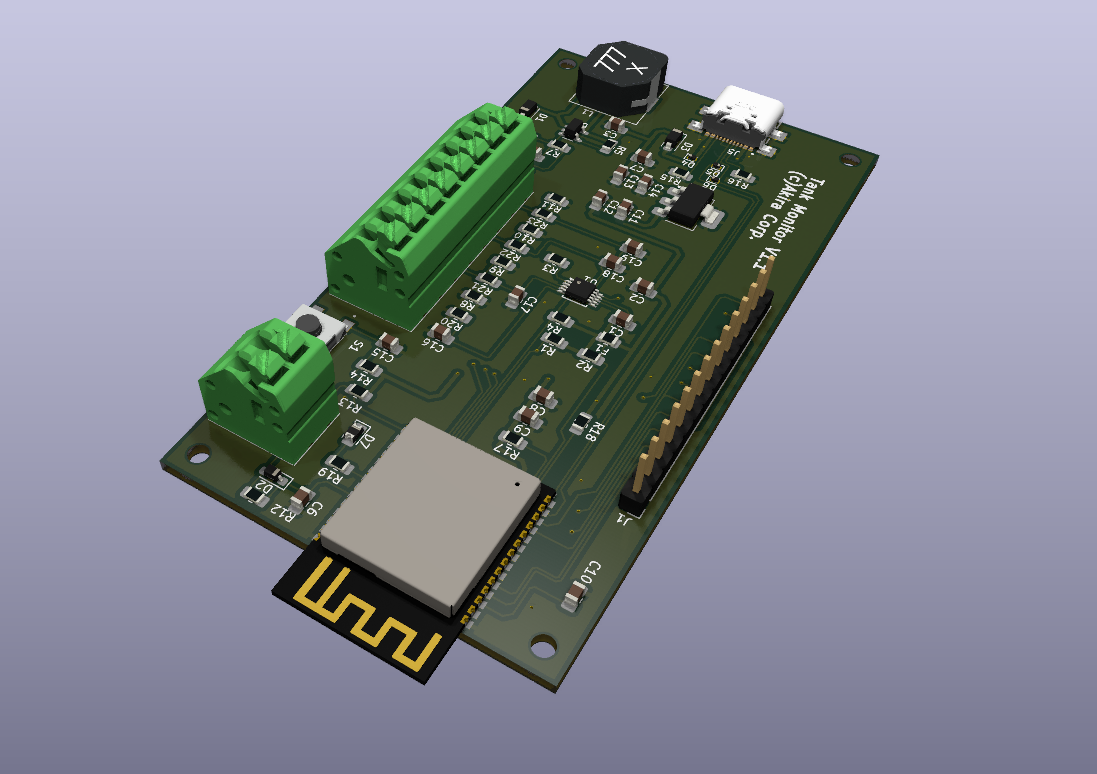
The design of the PCB has been done with KiCad 9.0. Particular footprint and 3D STEP file are included in the /footprints folder for sake of maintenance
The design is based on ESP32C6 WROOM with the following peripherials:
Component size has been selected to 0805, except ESD protective diodes that are smaller.
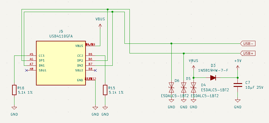
USB socket is grounded to the main ground planes (2 sides).
USB Lines USB- and USB+ are directly connected to ESP32C6 to flash and monitor µC.
VBUS is used to provide +5V (which is in fact lower than +5V) via a protective diode D3.
All this 3 lines are protected by ESD protective diode.
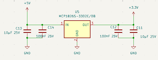
All the board is powered using +3.3V. This voltage is provided by a fixed low-voltage regulator MCP1826S-3302E that can provide up to 1000mA.
Fixed voltage regulator requires only few external component, in this case only capacitors are installed as per datasheet.
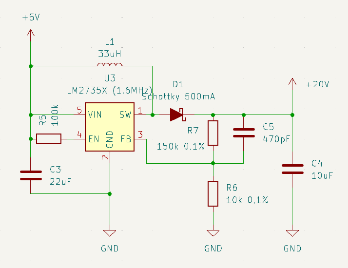
To avoid noise on lines and due to voltage drop at each stage, 4-20mA loop voltage shall be at around 20V. Care shall be taken when changing this voltage as it may require adjustment (in the shunt values for instance) to avoid damaging other components.
This voltage is produced from +5V using a boost type regulator LM2735X (@1.6MHz). Computation of the external components are provided in the LibreOffice Spreadsheet PCB comput spreadsheet. A 33µH inductance has been selected to get a clean output voltage to avoid noise on sensors line.
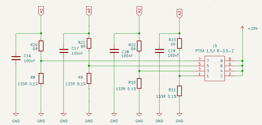
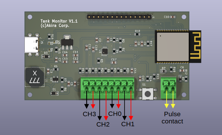
4 channels are available via Phoenix contact 8 poles connector. Each channel input current is injected in a 133R shunt (low tolerance resistor) to output a voltage below 3.3V. A 100nF capacitor is provided to reduce noise.
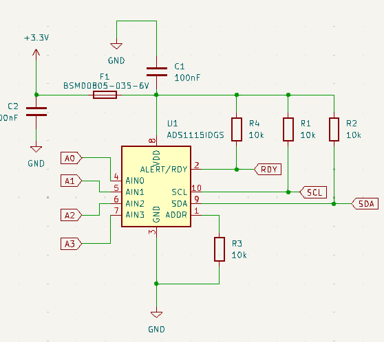
Each channel voltage is then converted in a digital signal using an ADS1115IDGS, that communicate with µC using i2c protocol. A ready pin is used to trigger an interrupt to the µC when data are available. External components are:
SCL, SDA, RDY) connected to µC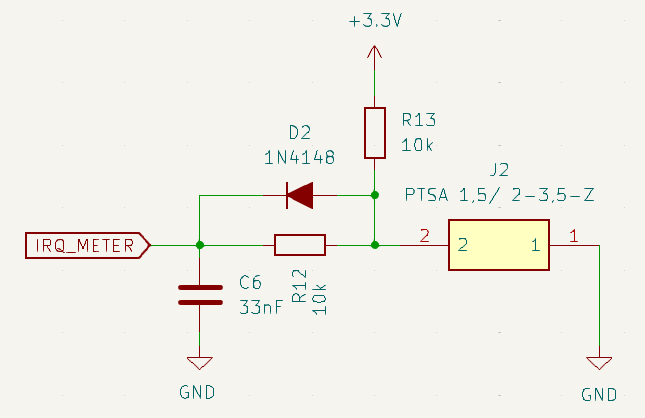
An harware RC filter has been set up on this input to avoid false triggering. The computation of this filter is detailed in the spreadsheet file PCB comput spreadsheet, bouncing duration has been measured using an oscilloscope in a unique water meter equiped with dry contact pulse output. It may be required to adjust this filter if the water meter seems to input false pulse to the µC.
The only other component is a pull-up resistor to not let a float input.
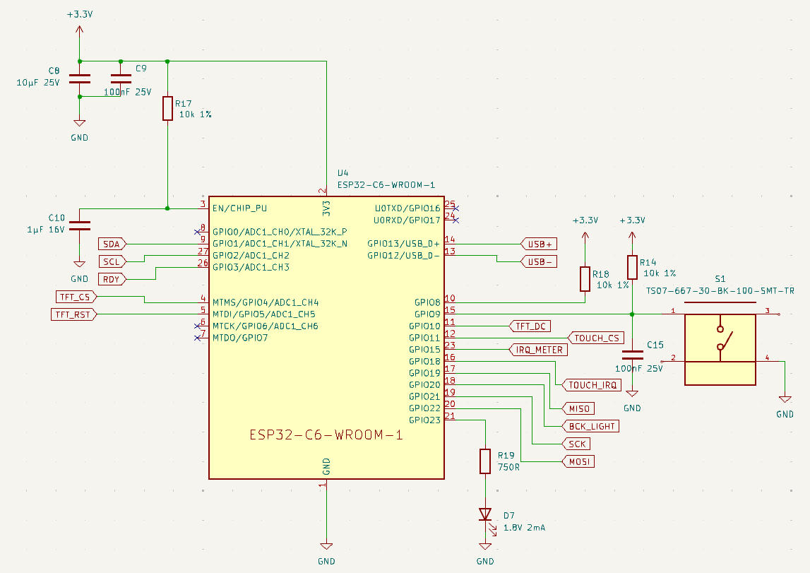
ESP32C6 power up is done using decoupling capacitor (10µF // 100nF).
The EN pin is driven to the +3.3V to enable the µC.
GPIO9 shall be pulled up to +3.3V to set the µC in normal execution mode (instead of ROM serial bootloader when GPIO9 is pulled to the ground). Despite the doc says that it has an internal pull-up, µC will not boot normally after reporg if not driven to +3.3V.
GPIO8 shall be driven to +3.3V as doc says, in order to enter the serial bootloader reliably.
Push button has been connected to GPIO9, so it can be used to boot/flash device by driving the pin low. Indeed, no operation is required on this button to flash µC using USB directly, and push button is used by software for HMI purpose.
A led is connected to GPIO23 for HMI purpose as well. Resistor has been calculated according to LED spec to grant the required current.
A header is available to drive a touchscreen if required. It has not been integrated in the enclosure of this repo. It was planned and tested using a ILI9341 TFT touchscreen.
Gerber files are included for fabrication. A batch of PCB has been produced by JLCPCB with the following configuration:
| Base Material | FR-4 | Layers | 2 |
|---|---|---|---|
| Dimension | 49 mm* 91 mm | PCB Qty | 20 |
| Product Type | Industrial/Consumer electronics | Different Design | 1 |
| Delivery Format | Single PCB | PCB Thickness | 1.6mm |
| Specify Stackup | no | Layer Sequence | |
| PCB Color | Purple | Silkscreen | White |
| Material Type | TG135 | Via Covering | Tented |
| Surface Finish | ENIG Gold Thickness: 1U" | Deburring/Edge rounding | No |
| Outer Copper Weight | 1 oz | Gold Fingers | No |
| Electrical Test | Flying Probe Fully Test | Castellated Holes | no |
| Edge Plating | No | Mark on PCB | Order Number |
| Blind Slot | No | Min via hole size/diameter | 0.3mm/(0.4/0.45mm) |
| 4-Wire Kelvin Test | No | Paper between PCBs | No |
| Appearance Quality | IPC Class 2 Standard | Confirm Production file | No |
| Silkscreen Technology | Ink-jet/Screen Printing Silkscreen | Package Box | With JLCPCB logo |
| Inspection Report | No | Board Outline Tolerance | ±0.2mm(Regular) |
| UL Marking | No | Countersink Hole | No |
A stencil as been produced by JLCPCB, so the assembly has been done using solder paste, manually placing components, and reflow is done using an hot plate.
The components that generate issues during that process are:
J5 : often some bridges are created due to the high density of pin. It has to be manually fixedD4, D5 & D6: are they are really small and light, they moved during the reflow process. It has to be manually fixed with a soldering iron, as hot air gun make them move anyway whaterver the airflow isU1(bridges) and µC U4 (alke of solder)J1, J2 and J3 have to be solded manuallyFor routing simplicity, 4-20mA channels are not reparted logically on the board, please consider the scheme here below.
Debounced pulse contact don't have polarity.
| Qty | Value | Footprint | References |
|---|---|---|---|
| 6 | 100nF | Capacitor_SMD:C_0805_2012Metric_Pad1.18x1.45mm_HandSolder | C1, C2, C16, C17, C18, C19 |
| 6 | 10k | Resistor_SMD:R_0805_2012Metric_Pad1.20x1.40mm_HandSolder | R1, R2, R3, R4, R12, R13 |
| 4 | 0R | Resistor_SMD:R_0805_2012Metric_Pad1.20x1.40mm_HandSolder | R20, R21, R22, R23 |
| 4 | 100nF 25V | Capacitor_SMD:C_0805_2012Metric_Pad1.18x1.45mm_HandSolder | C9, C12, C14, C15 |
| 4 | 10µF 25V | Capacitor_SMD:C_0805_2012Metric_Pad1.18x1.45mm_HandSolder | C7, C8, C11, C13 |
| 4 | 133R 0,1% | Resistor_SMD:R_0805_2012Metric_Pad1.20x1.40mm_HandSolder | R8, R9, R10, R11 |
| 3 | 10k 1% | Resistor_SMD:R_0805_2012Metric_Pad1.20x1.40mm_HandSolder | R14, R17, R18 |
| 3 | ESDALC5-1BT2 | Diode_SMD:D_SOD-882D | D4, D5, D6 |
| 2 | 5.1k 1% | Resistor_SMD:R_0805_2012Metric_Pad1.20x1.40mm_HandSolder | R15, R16 |
| 1 | 1.8V 2mA | Diode_SMD:D_0805_2012Metric_Pad1.15x1.40mm_HandSolder | D7 |
| 1 | 100k | Resistor_SMD:R_0805_2012Metric_Pad1.20x1.40mm_HandSolder | R5 |
| 1 | 10k 0,1% | Resistor_SMD:R_0805_2012Metric_Pad1.20x1.40mm_HandSolder | R6 |
| 1 | 10uF | Capacitor_SMD:C_0805_2012Metric_Pad1.18x1.45mm_HandSolder | C4 |
| 1 | 150k 0,1% | Resistor_SMD:R_0805_2012Metric_Pad1.20x1.40mm_HandSolder | R7 |
| 1 | 1N4148 | Diode_SMD:D_SOD-323_HandSoldering | D2 |
| 1 | 1N5819HW-7-F | Diode_SMD:D_SOD-123 | D3 |
| 1 | 1µF 16V | Capacitor_SMD:C_0805_2012Metric_Pad1.18x1.45mm_HandSolder | C10 |
| 1 | 22uF | Capacitor_SMD:C_0805_2012Metric_Pad1.18x1.45mm_HandSolder | C3 |
| 1 | 33nF | Capacitor_SMD:C_0805_2012Metric_Pad1.18x1.45mm_HandSolder | C6 |
| 1 | 33uH | Inductor_SMD:L_10.4x10.4_H4.8 | L1 |
| 1 | 470pF | Capacitor_SMD:C_0805_2012Metric_Pad1.18x1.45mm_HandSolder | C5 |
| 1 | 750R | Resistor_SMD:R_0805_2012Metric_Pad1.20x1.40mm_HandSolder | R19 |
| 1 | ADS1115IDGS | Package_SO:TSSOP-10_3x3mm_P0.5mm | U1 |
| 1 | BSMD0805-035-6V | Fuse:Fuse_0805_2012Metric | F1 |
| 1 | ESP32-C6-WROOM-1 | zTankFootprints:ESP32-C6-WROOM-1 | U4 |
| 1 | LM2735X (1.6MHz) | Package_TO_SOT_SMD:SOT-23-5 | U3 |
| 1 | MCP1826S-3302E/DB | Package_TO_SOT_SMD:SOT-223-3_TabPin2 | U5 |
| 1 | PTSA 1,5/ 2-3,5-Z | zTankFootprints:Phoenix Contact PTSA 2 | J2 |
| 1 | PTSA 1,5/ 8-3,5-Z | zTankFootprints:Phoenix Contact PTSA 8 | J3 |
| 1 | Schottky 500mA | Diode_SMD:D_SOD-123 | D1 |
| 1 | TFT | Connector_PinHeader_2.54mm:PinHeader_1x14_P2.54mm_Vertical | J1 |
| 1 | TS07-667-30-BK-100-SMT-TR | zTankFootprints:CUI switch SW_TS07-667-30-BK-100-SMT-TR | S1 |
| 1 | USB4110GFA | zTankFootprints:GCT_USB4110GFA | J5 |
The 60 most common of 64 parts.
bluedot-arcade/bd845-pwb-board
A clone of the original Konami GN845-PWB(B) Stage I/O board for DDR machines.


brokebit/SolarDataLogger
Firmware for custom data logger for Victron MPPT charge controllers via the Ve.Direct port/protocol.


Stan-debakker/grap-6TWEA
Daarnaast moest ik ervoor zorgen dat de nieuwe sensoren correct werken. Ik ben gestart met experimenteren via Arduino IDE, zie "codearduinoIDE".


JosueHerrera05/Josue_Herrera_Electiva_2026_C2
Repositorio Electíva Diseño Mecatrónico 2026-C2

It measures 49 × 91 mm and has 2 copper layers, 1.6 mm thick.
64 parts, built around the ESP32-C6-WROOM-1-N8, ADS1115IDGS, MCP1826S-3302E/DB and ESDALC5-1BT2Y. The full list of its parts is on this page, with links to each part's symbol and footprint where PCBKit's library has them.
From the akira215/zTank repository on GitHub, at the commit this page was made from: the board is PCB/tank_PCB.kicad_pcb and its schematic PCB/tank_PCB.kicad_sch. PCBKit opens the board in the browser, with nothing to install.
Its repository publishes it under the GPL-3.0 licence: you may reuse it on that licence's terms (keep the author's notice, and for a copyleft licence share your changes alike).