4 layers80 × 100 mm

 Aightech/CleverHand-hardware17
JACK CONN is an open-source printed circuit board by Aightech, from the Aightech/CleverHand-hardware repository on GitHub, published under the GPL-3.0 licence. It is a 4-layer board of 40.5 × 33 mm with 29 parts on 27 nets, routed with 71 tracks and 0 vias.
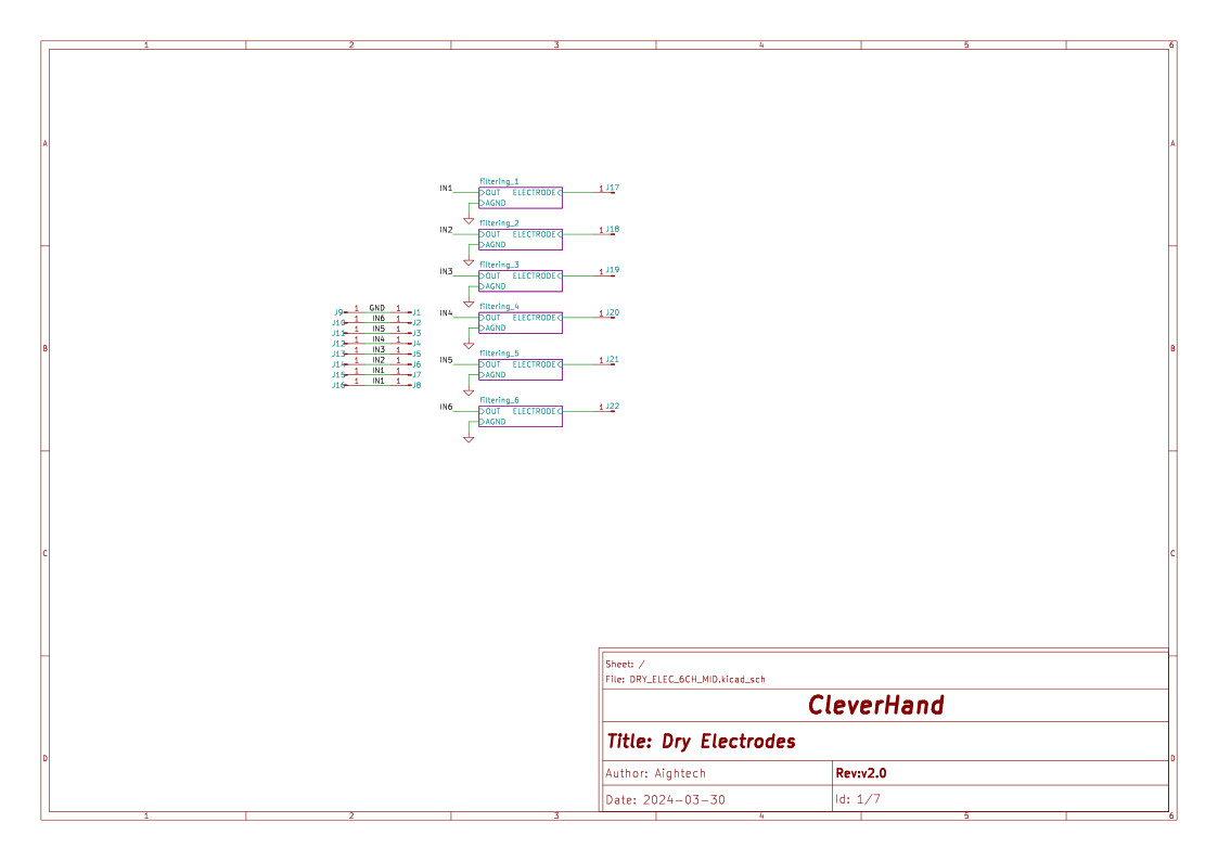
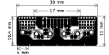
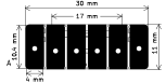
This module is responsible for interfacing the sensors/actuators inputs/outputs with the user skin or with other modules.
| top view | side view |
|---|---|
 |  |
| Qty | Value | Footprint | References |
|---|---|---|---|
| 16 | Conn_01x01_Pin | 00_custom-footprints:Pin_D1.2mm_pogo | J12, J13, J14, J15, J16, J17, J18, J19, J20, J21, J22, J23, J24, J25, J26, J27 |
| 9 | jack2.5_PJ-210B | 00_custom-footprints:Jack_Socket_PJ-210B | J1, J2, J3, J4, J5, J6, J7, J8, J9 |
| 2 | Conn_01x01_Pin | Connector_PinHeader_2.54mm:PinHeader_1x01_P2.54mm_Vertical | J10, J11 |
| 1 | G*** | kibuzzard-6607178A | kibuzzard-6607178A |
The 28 most common of 29 parts.


Hanqaqa/Easyduino
Easily dive into different PCB KiCad designs of the most popular microcontroller devboards


EvanKrall/pipad
A PCB for putting a Raspberry Pi CM4 inside a 1st-generation iPad.


alvarop/chaac
This is a work in progress for a wireless weather station project.


colinleroy/BurgerDisk
A daisy-chainable Smartport hard drive for the Apple II

esden/glasgow-addons
Various interface addon boards and expansions for the Glasgow Digital Interface Explorer
It measures 40.5 × 33 mm and has 4 copper layers, 0.8 mm thick.
29 parts. The full list of its parts is on this page, with links to each part's symbol and footprint where PCBKit's library has them.
From the Aightech/CleverHand-hardware repository on GitHub, at the commit this page was made from: the board is pcb/tool/extension/JACK_CONN/JACK_CONN.kicad_pcb. PCBKit opens the board in the browser, with nothing to install.
Its repository publishes it under the GPL-3.0 licence: you may reuse it on that licence's terms (keep the author's notice, and for a copyleft licence share your changes alike).