4 layers16.9 × 119.4 mm

 aguirrem/pcb-anatomy
examples/usb-blinky, drawn from its own .kicadpcb: every part at its package height, the +3V3 net lit with current flowing along it.
Usb blinky is an open-source printed circuit board by aguirrem, from the aguirrem/pcb-anatomy repository on GitHub. It is a 2-layer board of 32 × 24 mm with 17 parts on 19 nets, routed with 137 tracks and 19 vias.
It is built around the ATTINY85-20SU, AP2112K-3.3TRG1 and USB4105-GF-A. Its parts include 4 resistors, 3 capacitors, 2 ICs, 2 connectors and 1 diode. It belongs with the AVR (ATmega, ATtiny) boards of this library.


An agent skill for hardware: design boards in KiCad, review them, and draw them. Modelled on Anatomy, whose isometric figure kit it builds on.
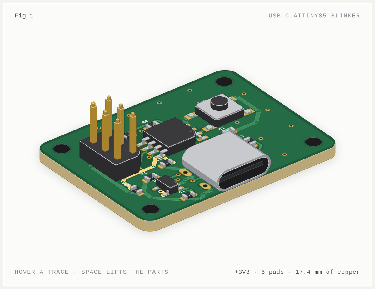
examples/usb-blinky, drawn from its own .kicad_pcb: every part at its package height, the +3V3 net lit with current flowing along it.
One skill, three modes:
| Mode | You ask for | You get |
|---|---|---|
| Design | "a USB-C powered ATtiny85 board, 32 × 24 mm, two layers, JLCPCB" | a KiCad 9/10 project built from one circuit spec: schematic (netlist parity and ERC clean), placed and autorouted board (DRC clean, ground stitched), renders, a self-review and fab outputs (Gerbers, drill, BOM, positions, IPC-2581, JLCPCB formats) |
| Review | "check this KiCad project before I order it" | a ranked report (blocker, major, minor, info) from ERC, DRC with schematic parity, fab limits, decoupling distances, floating inputs, current capacity, pair matching and BOM completeness, with every finding ringed on the board, plus the datasheet checks no script can do |
| Illustrate | "draw my board for the README" or "explain why decoupling caps sit by the pins" | an interactive isometric figure, from a real .kicad_pcb or an invented board built around the idea, in Anatomy's craft: solid parts, live readout from a true model, calm motion, checked in a headless browser |
git clone https://github.com/aguirrem/pcb-anatomy.git ~/.claude/skills/pcb-anatomy
bash ~/.claude/skills/pcb-anatomy/scripts/kicad/setup.sh      # KiCad 10, libraries, Java 25, Freerouting, headless Chrome
Then in Claude Code: /pcb-anatomy design a breakout board for the BME280, I2C, 3.3 V, castellated edges. In the Claude app, upload the folder as a skill (zip it with SKILL.md at the root). Claude also picks the skill up whenever you ask for anything PCB, schematic, KiCad, Gerber or hardware-figure shaped.
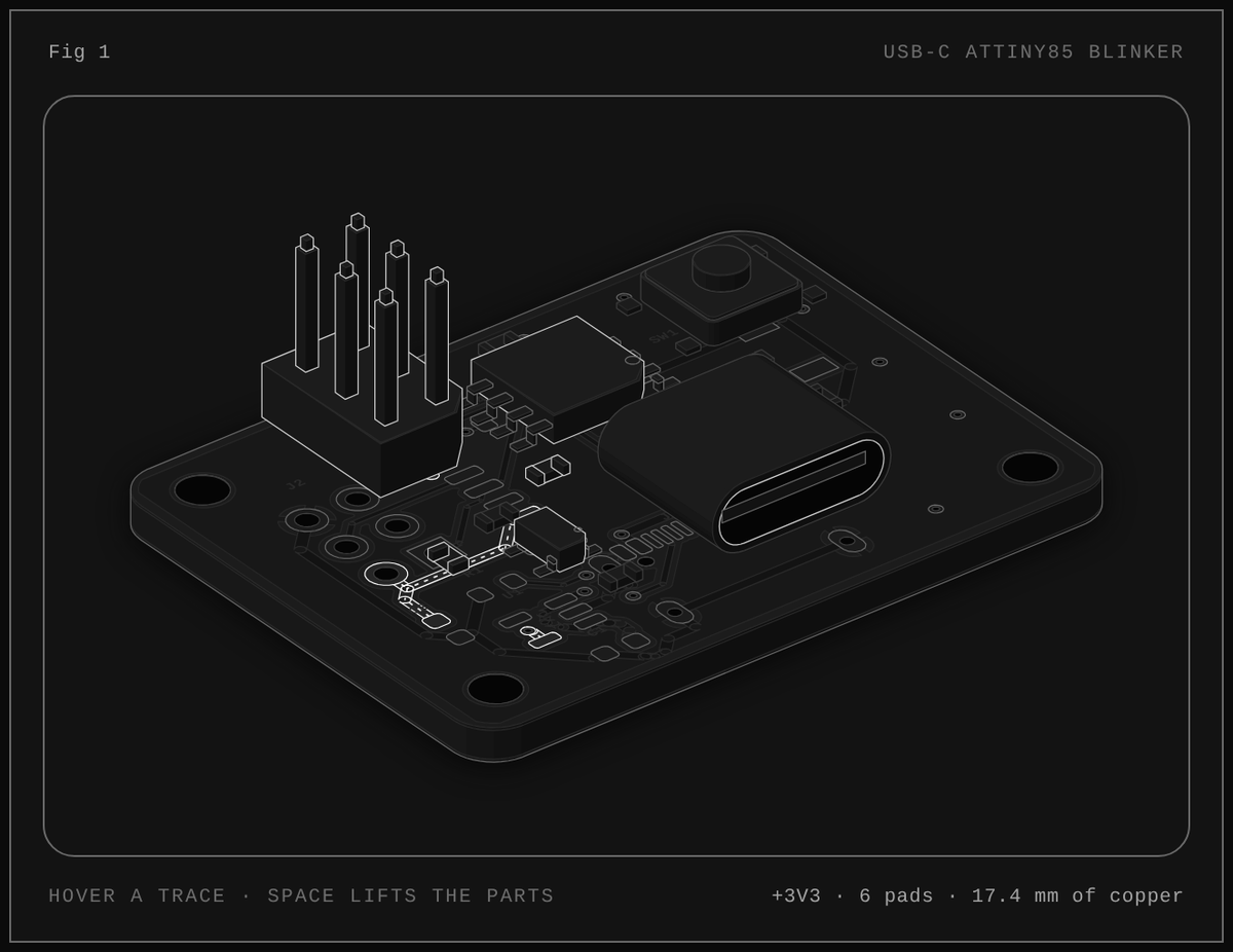 | 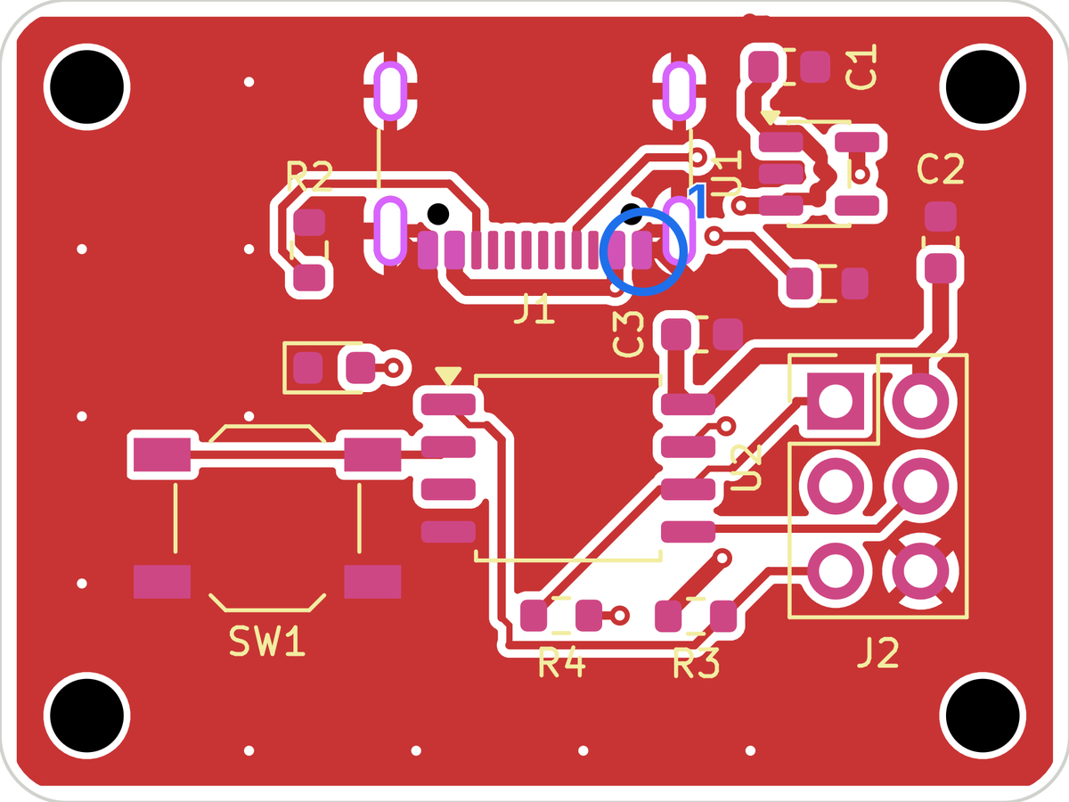 |
| Space lifts the parts off their pads on springs, so the copper under them shows. Monochrome "ink" palette. | Review: findings ringed and numbered on the board, matched to review.md. |
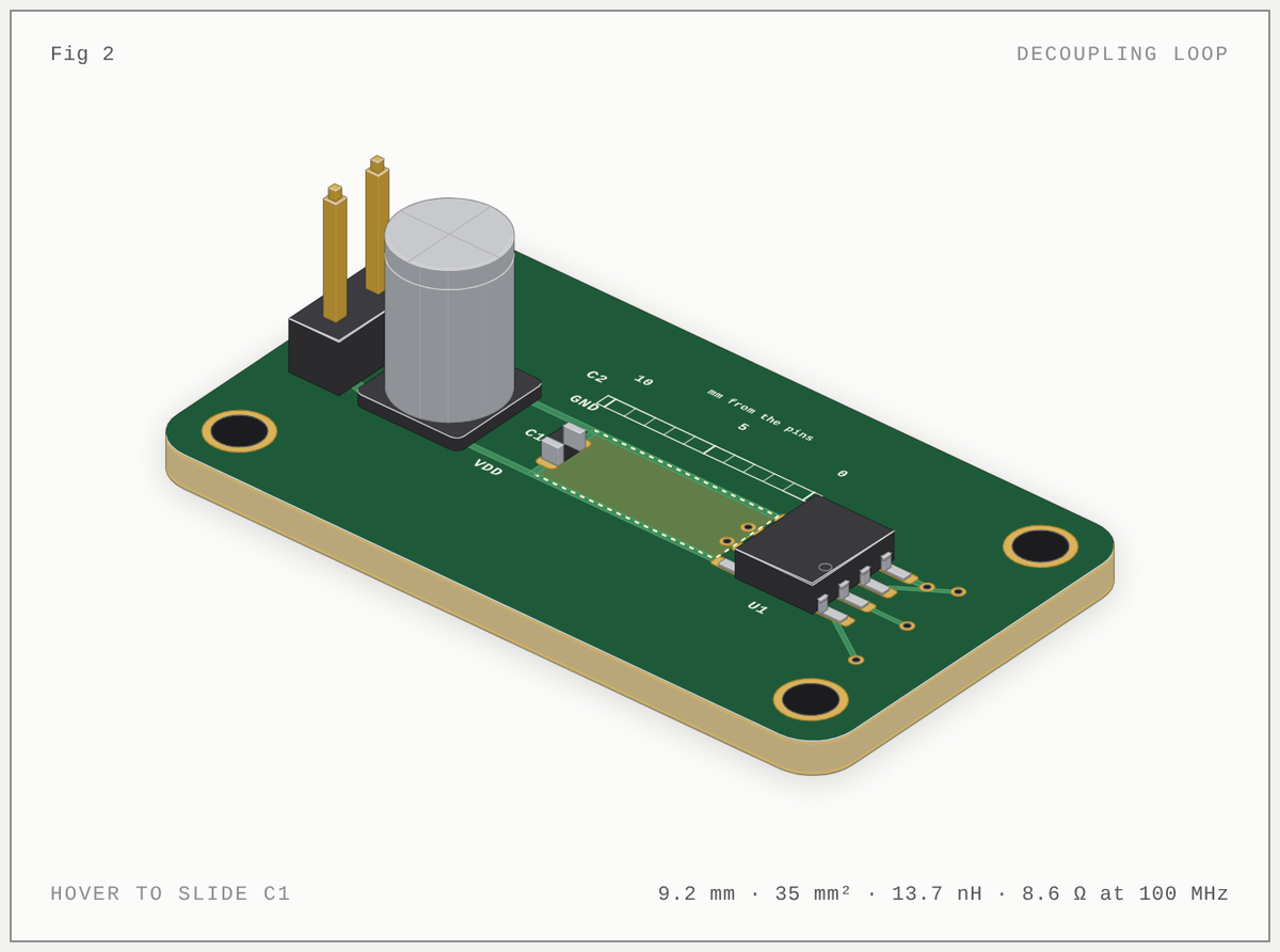 | 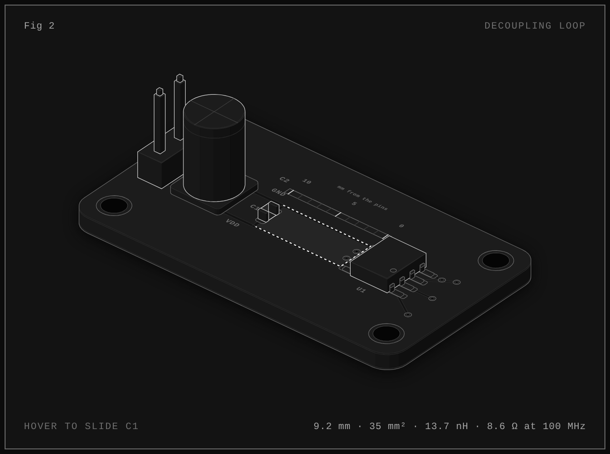 |
An idea figure: slide C1 along the rails and the loop it closes with the chip's supply pins grows; the readout gives its inductance and its impedance at 100 MHz from model.mjs. | The same, dark theme, ink palette. |
Design starts from a circuit spec (spec.yaml): parts as KiCad library symbols and footprints, nets as REF.PIN lists, deliberate no-connects, board size, rules, pours, and the placement of the parts that matter. sch_build.py writes the schematic and proves KiCad's netlist equals the spec; pcb_build.py builds the board from that netlist, places the anchors where the spec says and the passives next to what they serve (decoupling caps at supply pins); route.py routes with Freerouting, refills pours and stitches ground; outputs.py writes fab files and refuses a board that fails DRC. partgen.py makes symbols and IPC-7351 footprints for parts KiCad lacks. Every step renders PNGs, and the skill tells Claude to look at them.
Review (review.py) works on any KiCad 8–10 project. The script does the measurable checks; SKILL.md and references/review.md give Claude the second pass: datasheets, reference circuits, protection, dissipation, manufacturability.
Illustrate extends Anatomy's kit (vendored, MIT, in kit/anatomy/) with kit/pcb.mjs: boards, copper, pads, vias, and packages built from footprint geometry (chips with tinned caps, gull-wing ICs with bent leads, QFNs, headers, USB-C shells, nylon housings, tactile switches, axial and disc parts, electrolytics, LEDs). board_dump.py reads a real board; board-figure.mjs makes the interactive page. Invented boards are built in millimetres with the same parts, driven by a pure model.
pcb-anatomy/
├── SKILL.md                    what Claude reads: modes, workflow, rules
├── references/                 setup, spec format, design, parts, review, figures; anatomy/ (Anatomy's craft guides)
├── scripts/kicad/              setup.sh, find_part, sch_build, pcb_build, route, stitch, review, outputs,
│                               render, partgen, board_dump, and their helpers (sexp, spec, libsym, fplib, silk, kienv)
├── scripts/figure/             board-figure.mjs, and Anatomy's capture, drive and lines checks
├── kit/pcb.mjs                 PCB parts, palettes, boardFigure and its live script
├── kit/anatomy/                Anatomy's isometric kit, unchanged (MIT)
├── examples/usb-blinky/        a complete design: spec → schematic → board → review → fab → figure
├── examples/decoupling-loop/   an idea figure and its model
└── evals/evals.json test prompts and what a good answer containsKiCad 9 or 10 with kicad-cli and its Python module (design and review), Java 25 and Freerouting 2.5 (routing), Node.js 20.10+ and a headless Chrome (figures), PyYAML and librsvg. scripts/kicad/setup.sh installs or checks all of them on Linux and macOS and explains Windows; references/setup.md covers proxies, sandboxes and bundled-Python platforms.
--keep-tracks.MIT. The isometric kit in kit/anatomy/, the figure check scripts in scripts/figure/ (except board-figure.mjs and inline-kit.mjs) and the guides in references/anatomy/ come from Anatomy © 2026 Ryan, also MIT; see kit/anatomy/LICENSE. KiCad and Freerouting are installed separately under their own licences.
| Qty | Value | Footprint | References |
|---|---|---|---|
| 4 | MountingHole | MountingHole:MountingHole_2.2mm_M2 | H1, H2, H3, H4 |
| 2 | 1u | Capacitor_SMD:C_0603_1608Metric | C1, C2 |
| 2 | 5.1k | Resistor_SMD:R_0603_1608Metric | R1, R2 |
| 1 | 100n | Capacitor_SMD:C_0603_1608Metric | C3 |
| 1 | 10k | Resistor_SMD:R_0603_1608Metric | R3 |
| 1 | 330 | Resistor_SMD:R_0603_1608Metric | R4 |
| 1 | AP2112K-3.3 | Package_TO_SOT_SMD:SOT-23-5 | U1 |
| 1 | ATtiny85-20S | Package_SO:SOIC-8_5.3x5.3mm_P1.27mm | U2 |
| 1 | ISP | Connector_PinHeader_2.54mm:PinHeader_2x03_P2.54mm_Vertical | J2 |
| 1 | TL3342 | Button_Switch_SMD:SW_SPST_TL3342 | SW1 |
| 1 | USB4105-GF-A | Connector_USB:USB_C_Receptacle_GCT_USB4105-xx-A_16P_TopMnt_Horizontal | J1 |
| 1 | green | LED_SMD:LED_0603_1608Metric | D1 |


AndrewCraswell/agency
Native KiCad engineering prototype, separate from the earlier ESP32/tscircuit board. Open usb-scoring-platform.kicadpro in KiCad 10; schematic and PCB are the editable source, with no generator required.


It measures 32 × 24 mm and has 2 copper layers, 1.6 mm thick.
17 parts, built around the ATTINY85-20SU, AP2112K-3.3TRG1 and USB4105-GF-A. The full list of its parts is on this page, with links to each part's symbol and footprint where PCBKit's library has them.
From the aguirrem/pcb-anatomy repository on GitHub, at the commit this page was made from: the board is examples/usb-blinky/usb-blinky.kicad_pcb and its schematic examples/usb-blinky/usb-blinky.kicad_sch. PCBKit opens the board in the browser, with nothing to install.
Its repository states no licence, so its author keeps all rights: ask aguirrem before reusing the design.