
2 layers150 × 68 mm

 aestellic/mb-adv
GBA Multiboot Dongle
Mb adv 1.0 is an open-source printed circuit board by aestellic, from the aestellic/mb-adv repository on GitHub, published under the MIT licence. It is a 2-layer board of 57 × 54 mm with 10 parts on 42 nets, routed with 141 tracks and 8 vias.
It is built around the BOB-12009 and OS103011MS8QP1. Its parts include 3 ICs, 1 diode and 1 switch. It belongs with the RP2040 boards of this library.

[!WARNING] This project is a work-in-progress and is currently incomplete.
[!WARNING] The mb_adv is only compatible with certain devices. See COMPATIBILITY.md in the firmware repo for more info.
The mb_adv is a dongle for your GBA which injects multiboot ROMs via link cable.
With it, you can do stuff like shiny hunt Jirachi without being tethered to a Gamecube, boot Poké Transporter GB, and even connect your GBA to the internet!
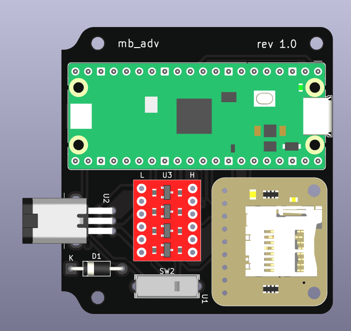
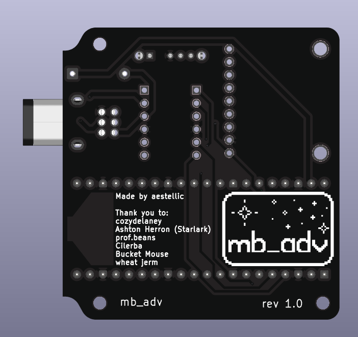
If you'd like to buy one and are located in the USA, you can visit my store here (link will be added when store goes live). Otherwise, please see MANUFACTURING.md for how to build one yourself!
See SETUP.md in the firmware repo.
How does this differ from the GB-Link?
What does mb_adv stand for?
What the heck is a multiboot?
How did you make this?

This project would not have been possible without the following people:
Note: the mb_adv is not endorsed by zaksabeast in any way, shape, or form.
This project is fully open sourced under the MIT License.
See MANUFACTURING.md and SCHEMATIC.pdf
| Qty | Value | Footprint | References |
|---|---|---|---|
| 3 | MountingHole_2.5mm | MountingHole:MountingHole_2.5mm | M2.5, M2.5, M2.5 |
| 1 | 1N5819 | Diode_THT:D_DO-41_SOD81_P10.16mm_Horizontal | D1 |
| 1 | Adafruit-MicroSD-SPI-4682 | adafruit:adafruit_4682 | U1 |
| 1 | BOB-12009 | BOB-12009:CONV_BOB-12009 | U3 |
| 1 | LOGO | logo:starry | G*** |
| 1 | RaspberryPi_Pico | Module:RaspberryPi_Pico_Common_THT | A1 |
| 1 | SW_SP3T | DIP4_SP3T-TOP_4P3X8P6_CNK:DIP4_SP3T-TOP_4P3X8P6_CNK | SW2 |
| 1 | gba_link_cable | GBA:GBALinkPort_Male | U2 |
It measures 57 × 54 mm and has 2 copper layers, 1.6 mm thick.
10 parts, built around the BOB-12009 and OS103011MS8QP1. The full list of its parts is on this page, with links to each part's symbol and footprint where PCBKit's library has them.
From the aestellic/mb-adv repository on GitHub, at the commit this page was made from: the board is mb_adv_1.0.kicad_pcb and its schematic mb_adv_1.0.kicad_sch. PCBKit opens the board in the browser, with nothing to install.
Its repository publishes it under the MIT licence: you may reuse it on that licence's terms (keep the author's notice, and for a copyleft licence share your changes alike).


agtbaskara/game-boy-pico-link-board
An Open-Source USB to Gameboy Link Cable Adapter for Raspberry Pi Pico


VincentKobz/diy-weather-station
The goal is to build from scratch a small intelligent weather station that can be connected to IOT networks.
