2 layers81.5 × 44 mm
AudioAmpEEL
ADolbyB/vlsi-spice-pcbs
A collection of Schematics, PCBs and VLSI work on various platforms
23 parts2

 ADolbyB/vlsi-spice-pcbs2
A collection of Schematics, PCBs and VLSI work on various platforms
Tutorial1 is an open-source printed circuit board by ADolbyB, from the ADolbyB/vlsi-spice-pcbs repository on GitHub. It is a 2-layer board of 52 × 35 mm with 4 parts on 4 nets, routed with 12 tracks and 0 vias.
It is built around the M2011S3A1W03. Its parts include 1 resistor, 1 diode and 1 switch.
This tutorial can be found in the help -> Getting Started With KiCad menu in the Schematic Editor of
KiCad.
This small tutorial covers schematic building, PCB layout, symbol & library creation, and 3D rendering. The KiCad files are arranged in the default manner.
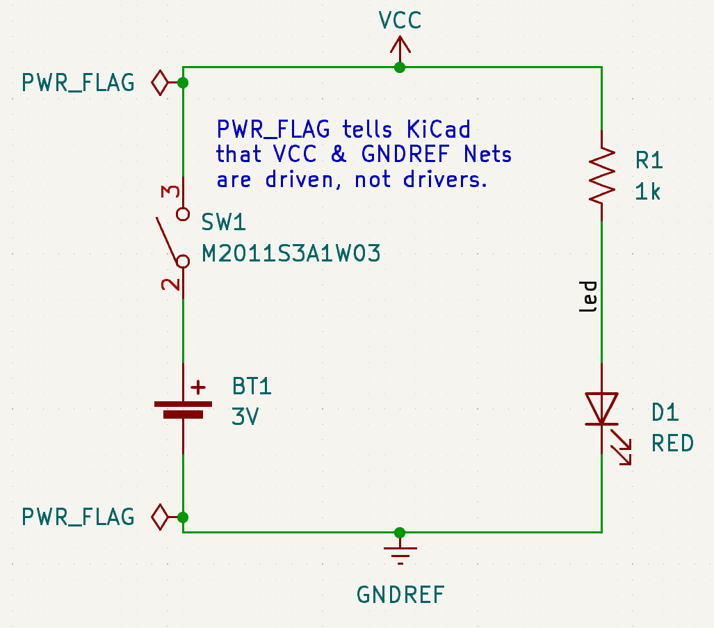
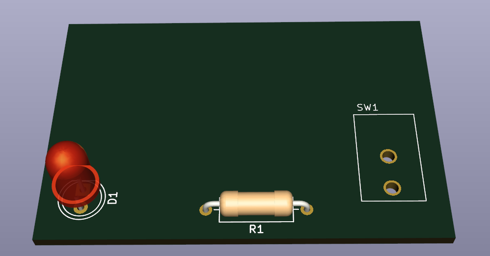
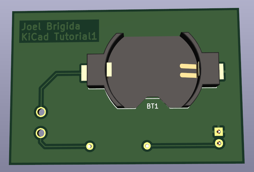
| Qty | Value | Footprint | References |
|---|---|---|---|
| 1 | 1k | Resistor_THT:R_Axial_DIN0309_L9.0mm_D3.2mm_P12.70mm_Horizontal | R1 |
| 1 | 3V | Battery:BatteryHolder_Keystone_1058_1x2032 | BT1 |
| 1 | M2011S3A1W03 | SPST_NKK:Switch_Toggle_SPST_NKK_M2011S3A1x03 | SW1 |
| 1 | RED | LED_THT:LED_D5.0mm | D1 |
ADolbyB/vlsi-spice-pcbs
A collection of Schematics, PCBs and VLSI work on various platforms


joypad-ai/joypad-os
Universal controller firmware for building adapters, dongles, and custom controllers.


hackclub/OnBoard
💡 Join 1,000 teenagers and make your first PCB with a $100 grant!

tardate/LittleArduinoProjects
a collection of "Little Electronic & Arduino Projects", most involving electronics or an Arduino in one way or another!
It measures 52 × 35 mm and has 2 copper layers, 1.6 mm thick.
4 parts, built around the M2011S3A1W03. The full list of its parts is on this page, with links to each part's symbol and footprint where PCBKit's library has them.
From the ADolbyB/vlsi-spice-pcbs repository on GitHub, at the commit this page was made from: the board is KiCAD/Tutorial1/Tutorial1.kicad_pcb and its schematic KiCAD/555-Badge/555_Badge.kicad_sch. PCBKit opens the board in the browser, with nothing to install.
Its repository states no licence, so its author keeps all rights: ask ADolbyB before reusing the design.