2 layers60 × 111.3 mm
Silkscreen pcb
iandchasse/silkscreen-pcb
Silkscreen: open-hardware ESP32-S3 e-paper reader mainboard (KiCad 9). Formerly the de-link hub.
189 parts589CERN-OHL-S-2.0
 ACodingGirrafe/kicad-projects1
kicad larp progress
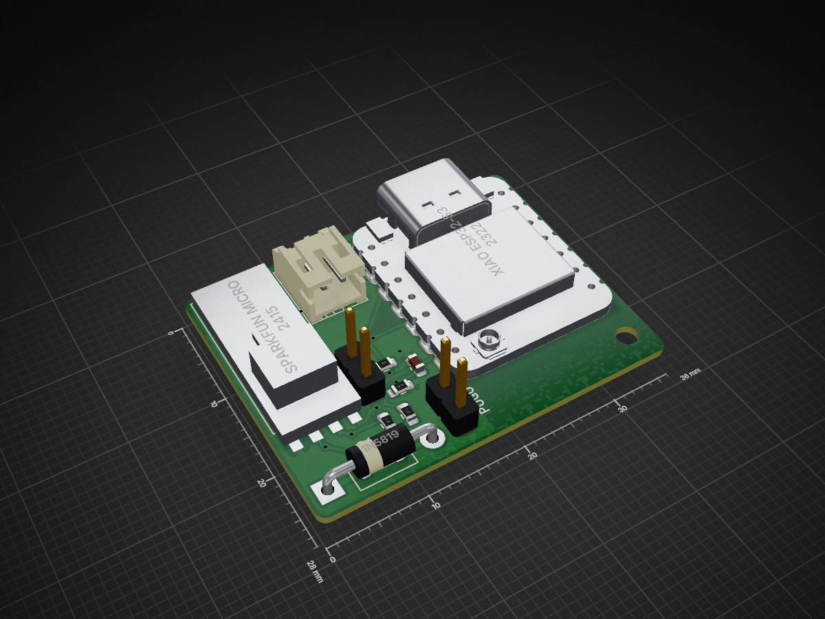
Swing pod is an open-source printed circuit board by ACodingGirrafe, from the ACodingGirrafe/kicad-projects repository on GitHub. It is a 2-layer board of 36 × 28 mm with 19 parts on 24 nets, routed with 88 tracks and 13 vias.
It is built around the 1N5819-T and S2B-PH-K-S(LF)(SN). Its parts include 4 resistors, 3 connectors, 2 ICs, 1 capacitor and 1 diode. It belongs with the ESP32 boards of this library.


An attempt to make PCB for a badminton swing-tracker pod for Jesus. A Seeed XIAO ESP32-S3 and a SparkFun Micro 6DoF IMU (LSM6DSV16X) sit on a 36 x 28 mm, 2-layer, 0.8 mm board. It charges through USB-C or through magnetic pogo pads. Made in KiCad 10.0.7.
| Path | What |
|---|---|
swing-pod.kicad_pro / .kicad_sch / .kicad_pcb | KiCad project |
outputs/swing-pod-schematic.pdf | Schematic |
outputs/swing-pod-gerbers-jlcpcb.zip | Gerbers + Excellon drill (PTH/NPTH), upload to JLCPCB as-is |
outputs/gerbers/ | Same files unzipped, plus drill maps |
outputs/swing-pod-bom.csv | BOM with manufacturer + MPN |
outputs/swing-pod-pos.csv | Pick-and-place, mm, absolute coordinates (board top-left = 100,100) |
outputs/swing-pod-assembly.pdf | Top assembly drawing (fab layer, all refdes) |
outputs/swing-pod-assembled.step | Assembled 3D model for the housing fit check |
outputs/renders/ | Top, bottom, 3D renders and outline SVG |
outputs/erc-report.rpt, drc-report.rpt | Final check reports |
lib/ | Project libraries (Seeed XIAO library, custom footprints, 3D models) |
tools/ | Scripts for the steps the KiCad MCP server can't do (see below) |
| From bottom of PCB to top of | Height |
|---|---|
| JST PH side-entry J1 (tallest part) | 5.65 mm |
| SparkFun module (1.6 mm PCB + Qwiic connector) | 5.36 mm |
| XIAO USB-C shell | 5.26 mm |
| XIAO shield | 4.05 mm |
| U.FL + mated plug (Hirose spec, 2.5 mm max mated) | about 4.6 mm |
5.65 mm is under the 6.0 mm budget. That assumes the through-hole leads (J1, D1, wire pads) are trimmed flush on the bottom. Untrimmed, the JST pins stick out 2.6 mm below the board.
Power netclass (VBAT, VUSB, POGO_P, GND): 0.5 mm tracks, 0.8/0.4 mm vias.ANTENNA_KEEPOUT (both layers, no copper): x 117.2–127, y 118–128. That is the XIAO's U.FL corner and the strip below it.IMU_UNDERSIDE (top layer only, no copper): under the flat-mounted SparkFun module's body.tools/check_netlist.py, plus a separate check of the PCB pad nets): all 9 nets PASS.| Spec line | Net | Pins |
|---|---|---|
| Battery + to XIAO BAT+ | VBAT | U1.23 (BAT+ pad), J1.1, J2.1, R1.1, TP5 |
| Battery − to XIAO BAT− | GND | U1.24 (BAT− pad), U1.13, U1.18, J1.2, J2.2, J3.2, U2.2, U2.6, R2.2, C1.2, TP2 |
| Pogo + to Schottky anode | POGO_P | J3.1 to D1.2 (A) |
| Schottky cathode to XIAO 5V | VUSB | D1.1 (K) to U1.14 (5V/VBUS), TP6 |
| Divider node to D2, 100 nF to GND | VBAT_SENSE | R1.2, R2.1, C1.1, U1.3 (D2/GPIO3), TP7 |
| IMU 3V3 and pull-ups to XIAO 3V3 | +3V3 | U1.12 (3V3), U2.1, R3.1, R4.1, TP1 |
| SDA | I2C_SDA | U2.3 to U1.5 (D4/GPIO5), R3.2, TP3 |
| SCL | I2C_SCL | U2.4 to U1.6 (D5/GPIO6), R4.2, TP4 |
| INT1 (deep-sleep wake) | IMU_INT1 | U2.5 to U1.2 (D1/GPIO2) |
XIAO pins used: D1 (GPIO2), D2 (GPIO3), D4 (GPIO5), D5 (GPIO6), 3V3, 5V, GND, plus the BAT+ and BAT− underside pads. Every other pin is marked no-connect. The GPIO mapping is checked against Seeed's wiki pin table.
I2C_PU). Your 4.7 kΩ R3/R4 in parallel give about 1.5 kΩ, which works fine. Either cut I2C_PU or leave R3/R4 unfitted.LED jumper to save about 0.7 mA in sleep.swing-pod:SparkFun_Micro_6DoF_LSM6DSV16X_Flat: built from SparkFun's Eagle board file (19.05 × 7.62 mm, test pads at 1.905 mm pitch, 0.7 mm holes enlarged to 0.8 mm).swing-pod:D_DO-41_P10.16mm_Horizontal_SOD-123_Alt: KiCad's DO-41 and SOD-123 land patterns merged into one footprint.swing-pod:WirePads_1x02_P3.0mm_D0.7mm: two plated wire pads for 26–30 AWG wire.lib/3d/SparkFun_Micro_6DoF.step: a simple box model, not SparkFun's.lib/3d/XIAO-ESP32S3.step: Seeed's official model, re-oriented to fit the footprint.XIAO-ESP32-S3-SMD) are Seeed's official files from their OPL KiCad library. They're unchanged except for the attached 3D model.tools/ holds the steps the KiCad MCP server couldn't do. Run them with KiCad's Python (or a venv built with --system-site-packages on top of it):
board_extras.py: keep-outs, and the BAT-pad vias open on the bottom.sync_fields.py: copies symbol fields, BOM flags and unconnected-net names to the PCB (the MCP sync skips them).make_3d_models.py: builds the XIAO and SparkFun 3D models. Needs pip install cadquery-ocp.check_netlist.py: compares the exported netlist against the connection spec. Run with any Python 3.| Qty | Value | Footprint | References |
|---|---|---|---|
| 2 | 4.7k | Resistor_SMD:R_0603_1608Metric | R3, R4 |
| 2 | 470k | Resistor_SMD:R_0603_1608Metric | R1, R2 |
| 1 | 100n | Capacitor_SMD:C_0603_1608Metric | C1 |
| 1 | 1N5819 | swing-pod:D_DO-41_P10.16mm_Horizontal_SOD-123_Alt | D1 |
| 1 | 3V3 | TestPoint:TestPoint_Pad_D1.0mm | TP1 |
| 1 | BAT+ | TestPoint:TestPoint_Pad_D1.0mm | TP5 |
| 1 | BATT JST-PH | Connector_JST:JST_PH_S2B-PH-K_1x02_P2.00mm_Horizontal | J1 |
| 1 | BATT PADS | swing-pod:WirePads_1x02_P3.0mm_D0.7mm | J2 |
| 1 | GND | TestPoint:TestPoint_Pad_D1.0mm | TP2 |
| 1 | M2 | MountingHole:MountingHole_2.2mm_M2 | H1 |
| 1 | POGO PADS | swing-pod:WirePads_1x02_P3.0mm_D0.7mm | J3 |
| 1 | SCL | TestPoint:TestPoint_Pad_D1.0mm | TP4 |
| 1 | SDA | TestPoint:TestPoint_Pad_D1.0mm | TP3 |
| 1 | SparkFun Micro 6DoF LSM6DSV16X | swing-pod:SparkFun_Micro_6DoF_LSM6DSV16X_Flat | U2 |
| 1 | VBAT_SENSE | TestPoint:TestPoint_Pad_D1.0mm | TP7 |
| 1 | VUSB | TestPoint:TestPoint_Pad_D1.0mm | TP6 |
| 1 | XIAO ESP32-S3 | Seeed_Studio_XIAO_Series:XIAO-ESP32-S3-SMD | U1 |
It measures 36 × 28 mm and has 2 copper layers, 0.8 mm thick.
19 parts, built around the 1N5819-T and S2B-PH-K-S(LF)(SN). The full list of its parts is on this page, with links to each part's symbol and footprint where PCBKit's library has them.
From the ACodingGirrafe/kicad-projects repository on GitHub, at the commit this page was made from: the board is projects/swing-pod/swing-pod.kicad_pcb and its schematic projects/js-drone/js_drone_pcb_rev_b_9_21.kicad_sch. PCBKit opens the board in the browser, with nothing to install.
Its repository states no licence, so its author keeps all rights: ask ACodingGirrafe before reusing the design.
iandchasse/silkscreen-pcb
Silkscreen: open-hardware ESP32-S3 e-paper reader mainboard (KiCad 9). Formerly the de-link hub.

chadaustin/wired-sculpt-pcb
KiCad design files for the Wired Sculpt conversion mod

klouderone/Kiwi36-Split
A 36 Key Split Keyboard for beginners packed full of features, such as USB-C interconnect, an extensive case library, and wireless support

Maritime-Hacking-Village/Badge-2025
Public repository for the official MHV 2025 badge.

cajunpanda/bluetooth-nes-advantage
A bluetooth mod for the NES Advantage classic controller.


RIVeR-Lab/BOOST
Multi-Agent Mission Concept for Battery Optimized Onsite Swapping Technology (BOOST)
