Skip to the content
2 layers42 × 33 mmSTM32 course, the printed circuit board in 3D

A beginner-friendly introduction to STM32 hardware design and KiCad

Size
42 × 33 mm
Copper layers
2
Thickness
1.6 mm
Parts
32
Nets
50
Pads
132
Tracks, vias
184, 25
Pours
4
Routed
Yes
KiCad
KiCad 10.0 (file 20260206)
Created
22 Aug 2026
Updated
22 Aug 2026

Overview

STM32 course is an open-source printed circuit board by abda-s, from the abda-s/STM32-Phill-s-Lab-PCB-Course repository on GitHub. It is a 2-layer board of 42 × 33 mm with 32 parts on 50 nets, routed with 184 tracks and 25 vias.

It is built around the STM32F103C8T6 and AMS1117-3.3. Its parts include 13 capacitors, 5 resistors, 4 connectors, 2 ICs and 1 diode. It belongs with the STM32 boards of this library.

Main components

2

README

README.md

STM32 Course PCB — V0.1

A beginner-friendly introduction to STM32 hardware design and KiCad. This is a minimal black-pill-style board built around the STM32F103C8T6 (ARM Cortex-M3), designed while following Phil's Lab's free full tutorial:

KiCad 6 STM32 PCB Design Full Tutorial — Phil's Lab #65 A ~1h40m step-by-step walkthrough of an STM32-based PCB — schematic creation, two-layer layout and routing, through to manufacturing files.

This project is just a beginner intro to STM32 hardware design and KiCad — the design is intentionally kept simple (no ESD protection, no fancy features) while following good design practices taught in the course. It is a learning project, not production-ready hardware.

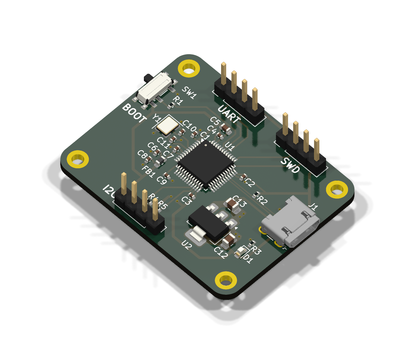
3D render — orthographic 3/4 isometric

Features

  • MCU: STMicroelectronics STM32F103C8T6 (Cortex-M3, 48-pin)
  • Power supply: AMS1117-3.3 linear regulator, powered from USB (5V VBUS)
  • USB: Micro-B connector, device-only USB-FS design
  • Clock: 8 MHz crystal with load capacitors
  • Debug/IO: SWD header, I2C bus with pull-ups
  • 4x mounting holes

Course Overview

The video covers the complete PCB design workflow in three stages. This project follows it end to end:

1. Schematic

  • STM32 microcontroller & decoupling — one 100nF cap per VDD/VBAT pin, based on ST recommendations
  • Configuration pins — BOOT0 (run vs. bootloader mode) and NRST behavior
  • Pin-out planning with STM32CubeIDE
  • Crystal circuitry — load capacitor calculation from the crystal's CL spec
  • USB — device-only design, D+ pull-up resistor per AN4879, differential pair routing
  • Power supply & connectors — AMS1117-3.3 LDO, ferrite bead for the analog rail, USB Micro-B
  • Electrical Rules Check (ERC) and annotation
  • Footprint assignment

2. Layout

  • PCB set-up — two-layer board stackup, track/via sizes, grid settings
  • Placing the MCU with decoupling caps and crystal close by first
  • USB and SWD layout
  • Changing footprints, adding 3D models
  • Switch & connector placement, power supply layout
  • Mounting holes and board outline

3. Routing & Manufacturing

  • Decoupling and crystal routing first (short traces)
  • Signal routing, then power routing
  • Finishing touches and Design Rules Check (DRC)
  • Producing manufacturing files: BOM, CPL, Gerber, drill (e.g. for JLCPCB assembly)

Documentation

FileDescription
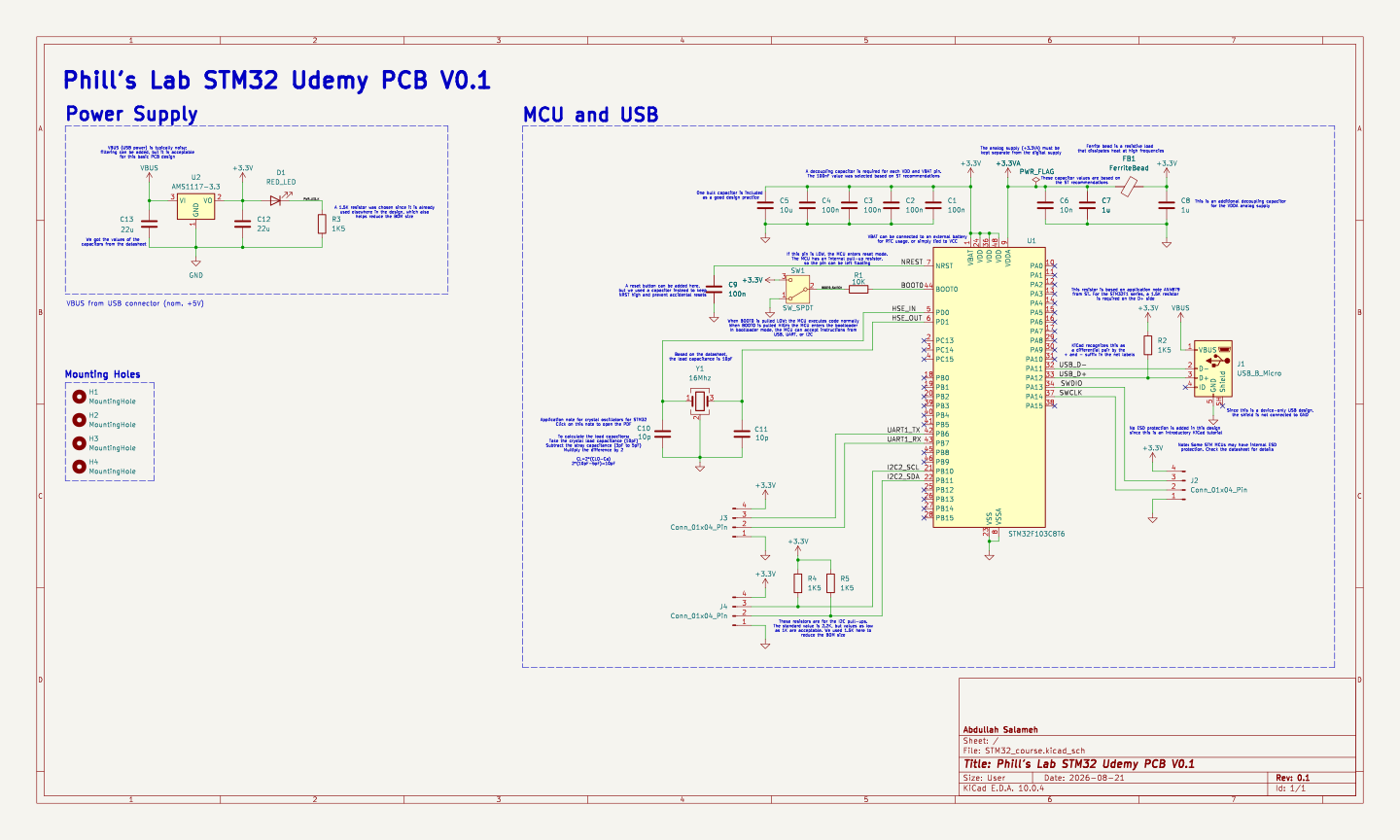
docs/schematic.pdfFull schematic (PDF)
docs/schematic.svgSchematic (SVG, viewable in browser)
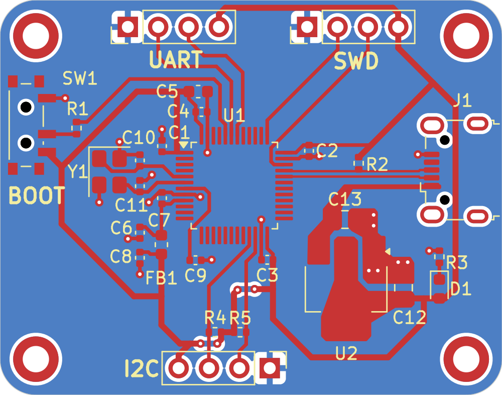
docs/pcb_overlay.pngPCB layout — both layers overlaid (F.Cu red, B.Cu blue)
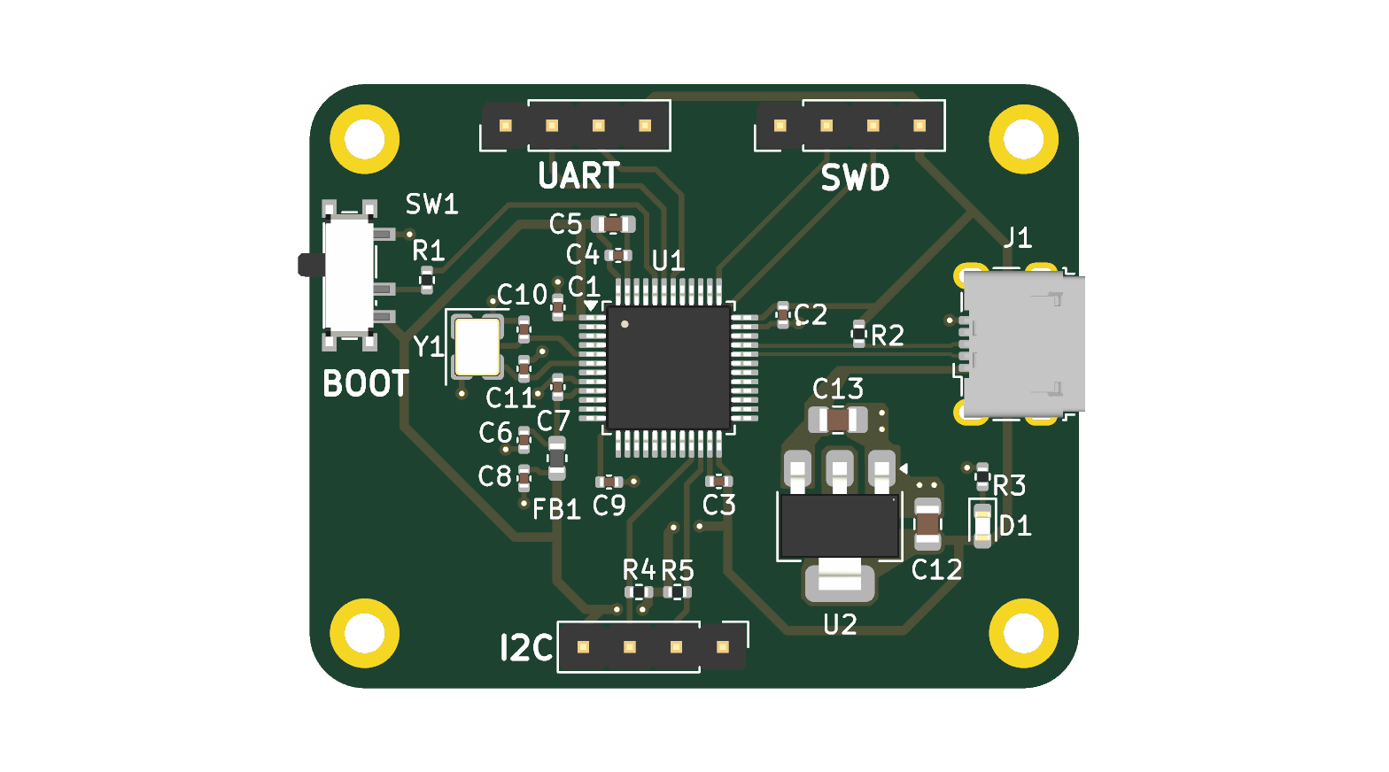
docs/pcb_3d_front.png3D render — top
docs/pcb_3d_iso.png3D render — orthographic 3/4 isometric

Schematic

Schematic

PCB Layout

Both copper layers overlaid — top (F.Cu, red) and bottom (B.Cu, blue) shown together:

PCB both layers overlaid

3D Render — Top View

3D render top

Design Notes

These are the notes taken directly on the schematic during the design process:

Power Supply

  • Capacitor values for the regulator were taken from the datasheet.
  • A bulk capacitor is included as good design practice.
  • The ferrite bead is a resistive load that dissipates heat at high frequencies.
  • VBUS (USB power) is typically noisy; filtering could be added but is acceptable for this basic PCB.

Decoupling

  • One decoupling capacitor per VDD and VBAT pin; 100nF selected based on ST recommendations.
  • The analog supply (+3.3VA) is kept separate from the digital supply via a ferrite bead, with an additional decoupling capacitor for VDDA.

MCU Configuration

  • BOOT0: pulled LOW → MCU executes code normally; pulled HIGH → MCU enters bootloader (can accept instructions over USB, UART, or I2C).
  • NRST: pin is LOW when in reset. The MCU has an internal pull-up, so it can be left floating. A reset button could be added here, but a capacitor was used instead to keep NRST high and prevent accidental resets.
  • VBAT: can be connected to an external battery for RTC usage, or simply tied to VCC.

Crystal Oscillator

  • Load capacitance calculation: take the crystal's load capacitance (10pF), subtract stray capacitance (~3–5pF), multiply by 2 → CL = 2 × (CL0 − Ca) = 2 × (10pF − 5pF) = 10pF.
  • Reference: ST oscillator design guide (AN2867)

USB

  • The 1.5K resistor on D+ is based on application note AN4879 from ST — required for the STM32F1 series. The 1.5K value was also chosen because it's already used elsewhere in the design, reducing BOM size.
  • This is a device-only USB design, so the cable shield is not connected to GND.
  • No external ESD protection is included since this is an introductory tutorial project (some STM MCUs may have internal ESD protection — check the datasheet).
  • USB differential pair routing: KiCad recognizes the pair by the + / - suffix in net labels.

I2C Pull-ups

  • Standard pull-up value is 2.2K, values as low as 1K are acceptable. 1.5K was used here to reduce the BOM size.

Status

This repository contains the completed PCB (V0.1) following the full tutorial above.

Tools

  • KiCad 10.x (the course itself uses KiCad 6, but the workflow is nearly identical)
  • STM32CubeIDE for pin-out planning

Parts

32
QtyValueFootprintReferences
5100nCapacitor_SMD:C_0402_1005MetricC1, C2, C3, C4, C9
41K5Resistor_SMD:R_0402_1005MetricR2, R3, R4, R5
4MountingHoleMountingHole:MountingHole_2.2mm_M2_DIN965_PadH1, H2, H3, H4
3Conn_01x04_PinConnector_PinHeader_2.54mm:PinHeader_1x04_P2.54mm_VerticalJ2, J3, J4
210pCapacitor_SMD:C_0402_1005MetricC10, C11
21uCapacitor_SMD:C_0402_1005MetricC7, C8
110KResistor_SMD:R_0402_1005MetricR1
110nCapacitor_SMD:C_0402_1005MetricC6
110uCapacitor_SMD:C_0603_1608MetricC5
116MhzCrystal:Crystal_SMD_3225-4Pin_3.2x2.5mmY1
122uCapacitor_SMD:C_0805_2012MetricC12
122uCapacitor_SMD:C_0805_2012Metric_Pad1.18x1.45mm_HandSolderC13
1AMS1117-3.3Package_TO_SOT_SMD:SOT-223-3_TabPin2U2
1FerriteBeadInductor_SMD:L_0603_1608MetricFB1
1RED_LEDLED_SMD:LED_0603_1608MetricD1
1STM32F103C8T6Package_QFP:LQFP-48_7x7mm_P0.5mmU1
1SW_SPDTButton_Switch_SMD:SW_SPDT_PCM12SW1
1USB_B_MicroConnector_USB:USB_Micro-B_Wuerth_629105150521J1

Similar boards

  • 2 layers68 × 40 mmStm32-io extend, the printed circuit board in 3D

    Stm32-io extend

    hardenedlinux/cheap-pcb

    Cheap PCB: Better understanding the current status of hardware supply chain

    44 parts170CC0-1.0
  • 2 layers99.1 × 58.4 mmHEAT, the printed circuit board in 3D

    HEAT

    milar111/HEAT

    An open-source STM32 SMD assembly station for precision soldering. Uses a custom Smart Pulse & Coast algorithm to drive 400W mains heaters via SSR. Features OLED UI, NTC feedback, and safety cooling.

    57 parts9
  • 2 layers71.3 × 25.4 mmUSB DALI, the printed circuit board in 3D

    USB DALI

    even-notodd/USB-DALI

    USB-DALI interface converter

    43 parts4
  • 2 layers78 × 60 mmDC Motor Controller, the printed circuit board in 3D

    DC Motor Controller

    minhle4397/Line-Follower-Robot-v2

    Improved Hardware and Firmware for Line Follower Robot

    53 parts3
  • 4 layers36 × 36 mmTrackMAG, the printed circuit board in 3D

    TrackMAG

    mupfdev/TrackMAG

    An open hardware development board primarily intended for the development of accessible input devices.

    58 parts3
  • 2 layers154.7 × 113 mmDeskMixer, the printed circuit board in 3D

    DeskMixer

    RaduAndre/DeskMixer

    DeskMixer is a software that allows control of application volumes with real sliders, and action mapping on buttons using arduino like platforms. The project was inspired originally by deej.

    113 parts3
  • 2 layers53.3 × 35.6 mmStm32 minimal dev, the printed circuit board in 3D

    Stm32 minimal dev

    amrithHN/stm32_minimal_dev

    stm32 based minimal dev board

    33 parts2GPL-3.0
  • 4 layers42 × 42 mmStepper Servo, the printed circuit board in 3D

    Stepper Servo

    jawher-Mansour/619-J_Stepper

    619-J_Stepper is an open source closed loop stepper driver.

    69 parts2

Questions

How big is the STM32 course PCB?

It measures 42 × 33 mm and has 2 copper layers, 1.6 mm thick.

What parts does the STM32 course use?

32 parts, built around the STM32F103C8T6 and AMS1117-3.3. The full list of its parts is on this page, with links to each part's symbol and footprint where PCBKit's library has them.

Where can I download the STM32 course KiCad files?

From the abda-s/STM32-Phill-s-Lab-PCB-Course repository on GitHub, at the commit this page was made from: the board is STM32_course.kicad_pcb and its schematic STM32_course.kicad_sch. PCBKit opens the board in the browser, with nothing to install.

Can I use the STM32 course design in my own project?

Its repository states no licence, so its author keeps all rights: ask abda-s before reusing the design.