4 layers71 × 83 mm

 aarthirethinabala/ESP32-Dev-Board
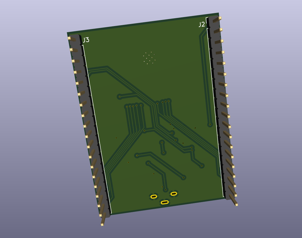
Custom ESP32 development board designed and routed in KiCad.
ESP32-Dev Board is an open-source printed circuit board by aarthirethinabala, from the aarthirethinabala/ESP32-Dev-Board repository on GitHub. It is a 2-layer board of 38.3 × 50 mm with 36 parts on 69 nets, routed with 361 tracks and 31 vias.
It is built around the ESP32-WROOM-32D, AMS1117-3.3 and ESD9B5.0ST5G, with the SS8050 and BAT60A among its other parts. Its parts include 11 resistors, 9 capacitors, 6 diodes, 3 ICs and 3 connectors. It belongs with the microcontroller boards boards and the ESP32 boards of this library.


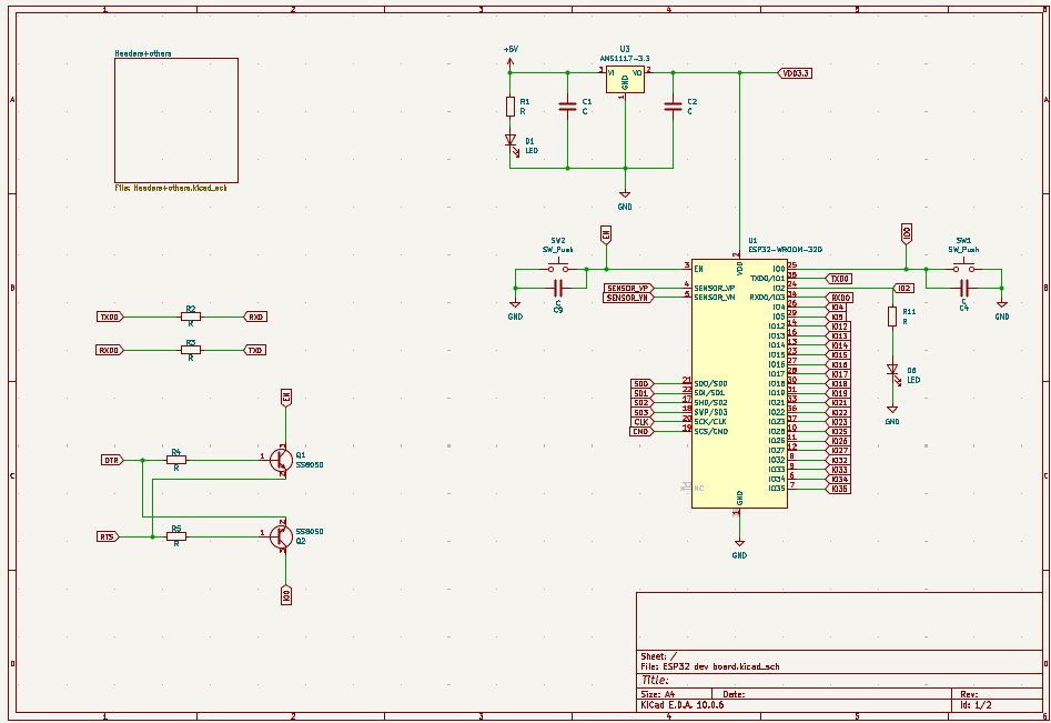
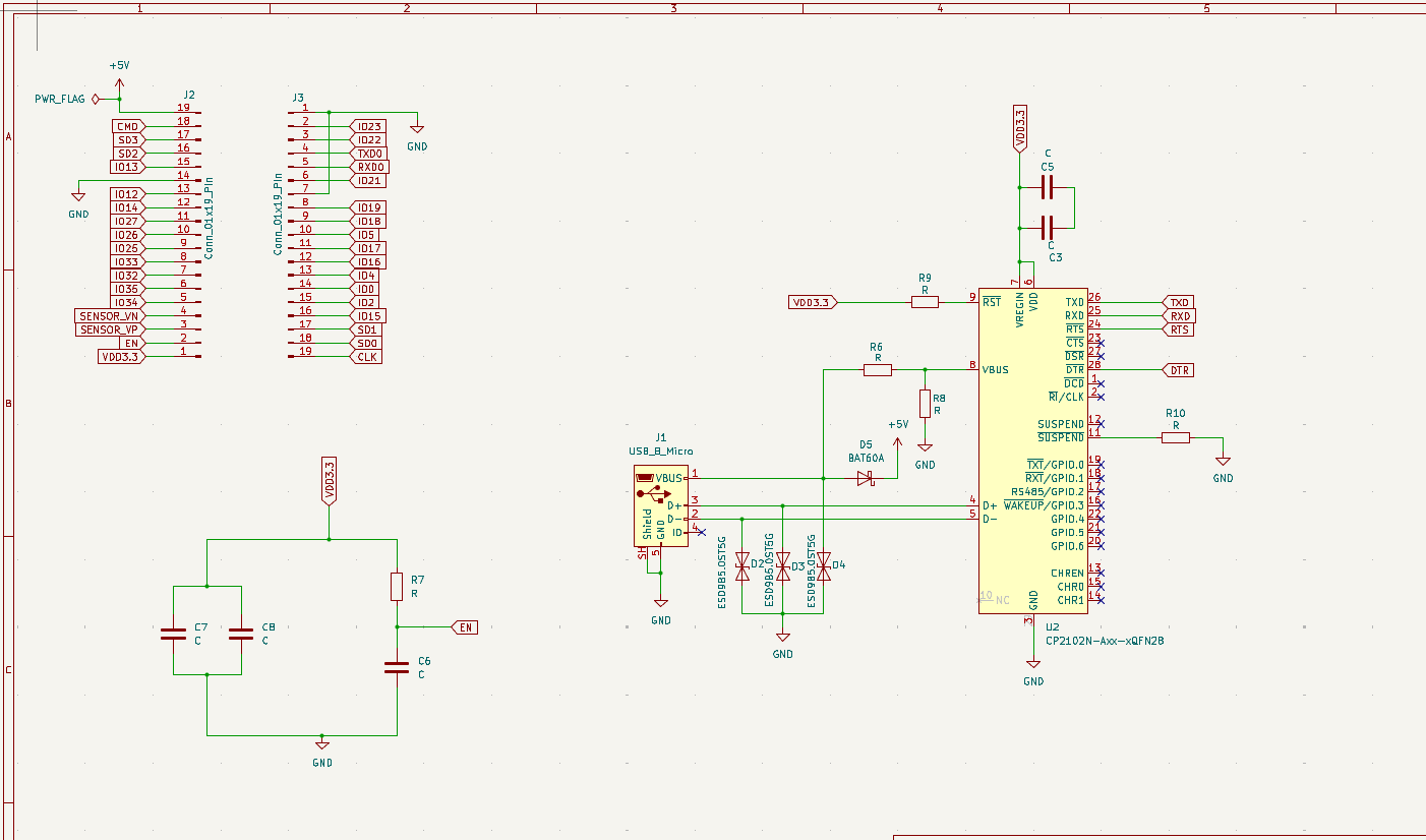
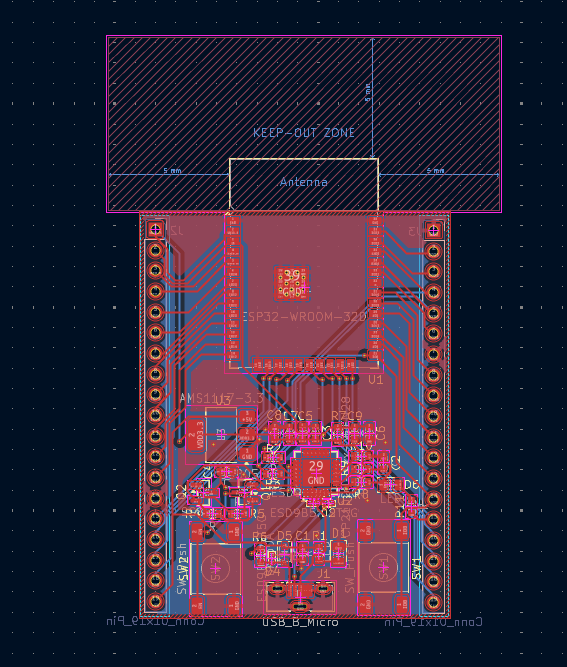
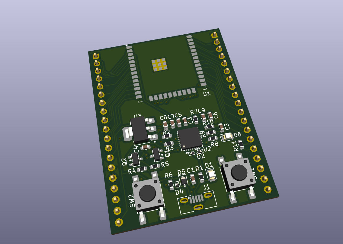
Custom ESP32 development board designed and routed in KiCad, including schematic design, component footprint assignment, PCB layout, routing and 3D visualization.
Completed
This project is a custom ESP32 development board based on the ESP32-WROOM module. The board was designed from the schematic stage through PCB layout and routing, including power regulation, USB-to-UART communication, boot/reset controls, GPIO headers, and supporting components.
| Qty | Value | Footprint | References |
|---|---|---|---|
| 11 | R | Resistor_SMD:R_0603_1608Metric | R1, R2, R3, R4, R5, R6, R7, R8, R9, R10, R11 |
| 9 | C | Capacitor_SMD:C_0603_1608Metric | C1, C2, C3, C4, C5, C6, C7, C8, C9 |
| 3 | ESD9B5.0ST5G | Diode_SMD:D_SOD-923 | D2, D3, D4 |
| 2 | Conn_01x19_Pin | Connector_PinHeader_2.54mm:PinHeader_1x19_P2.54mm_Vertical | J2, J3 |
| 2 | LED | LED_SMD:LED_0805_2012Metric | D1, D6 |
| 2 | SS8050 | Package_TO_SOT_SMD:SOT-23 | Q1, Q2 |
| 2 | SW_Push | Button_Switch_SMD:SW_Push_1P1T_NO_E-Switch_TL3301NxxxxxG | SW1, SW2 |
| 1 | AMS1117-3.3 | Package_TO_SOT_SMD:SOT-223-3_TabPin2 | U3 |
| 1 | BAT60A | Diode_SMD:D_SOD-323 | D5 |
| 1 | CP2102N-Axx-xQFN28 | Package_DFN_QFN:QFN-28-1EP_5x5mm_P0.5mm_EP3.35x3.35mm | U2 |
| 1 | ESP32-WROOM-32D | RF_Module:ESP32-WROOM-32D | U1 |
| 1 | USB_B_Micro | Connector_USB:USB_Micro-B_Molex-105133-0001 | J1 |
It measures 38.3 × 50 mm and has 2 copper layers, 1.6 mm thick.
36 parts, built around the ESP32-WROOM-32D, AMS1117-3.3, ESD9B5.0ST5G and SS8050. The full list of its parts is on this page, with links to each part's symbol and footprint where PCBKit's library has them.
From the aarthirethinabala/ESP32-Dev-Board repository on GitHub, at the commit this page was made from: the board is KiCad-Files/ESP32 dev board.kicad_pcb and its schematic KiCad-Files/ESP32 dev board.kicad_sch. PCBKit opens the board in the browser, with nothing to install.
Its repository states no licence, so its author keeps all rights: ask aarthirethinabala before reusing the design.

emiirkaya/ThermovitalSync-PCB
A PCB project for a vital monitoring-cooling device with GUI


akbar-q/Circuits-PCB-HardwareDesign
The High Voltage Arc Detector is a non-contact RF-based sensing system that detects high-voltage electrical arcs.


shukranwambua-maker/Code_and_ShortCircuits
"Those who don't INNOVATE perish!!!!!" - Muchai Wambua