
2 layers22.2 × 46.4 mm
C64-Switchless Quad Kernal Switcher
bwack/C64-Switchless-Multi-Kernal-27C256-adapter
Kernal switcher for the C64/C64C/C128
14 parts112

 AaronC81/attiny-breakout2
ISP breakout for ATTiny25/45/85
Attiny85-breakout is an open-source printed circuit board by AaronC81, from the AaronC81/attiny-breakout repository on GitHub. It is a 2-layer board of 22.9 × 21.6 mm with 4 parts on 8 nets, routed with 27 tracks and 0 vias.
It is built around the ATTINY85-20PU. Its parts include 3 connectors and 1 IC. It belongs with the interfaces and adapters boards and the AVR (ATmega, ATtiny) boards of this library.
This is a little breakout board for easy programming of DIP ATtiny25/45/85 chips on a breadboard.
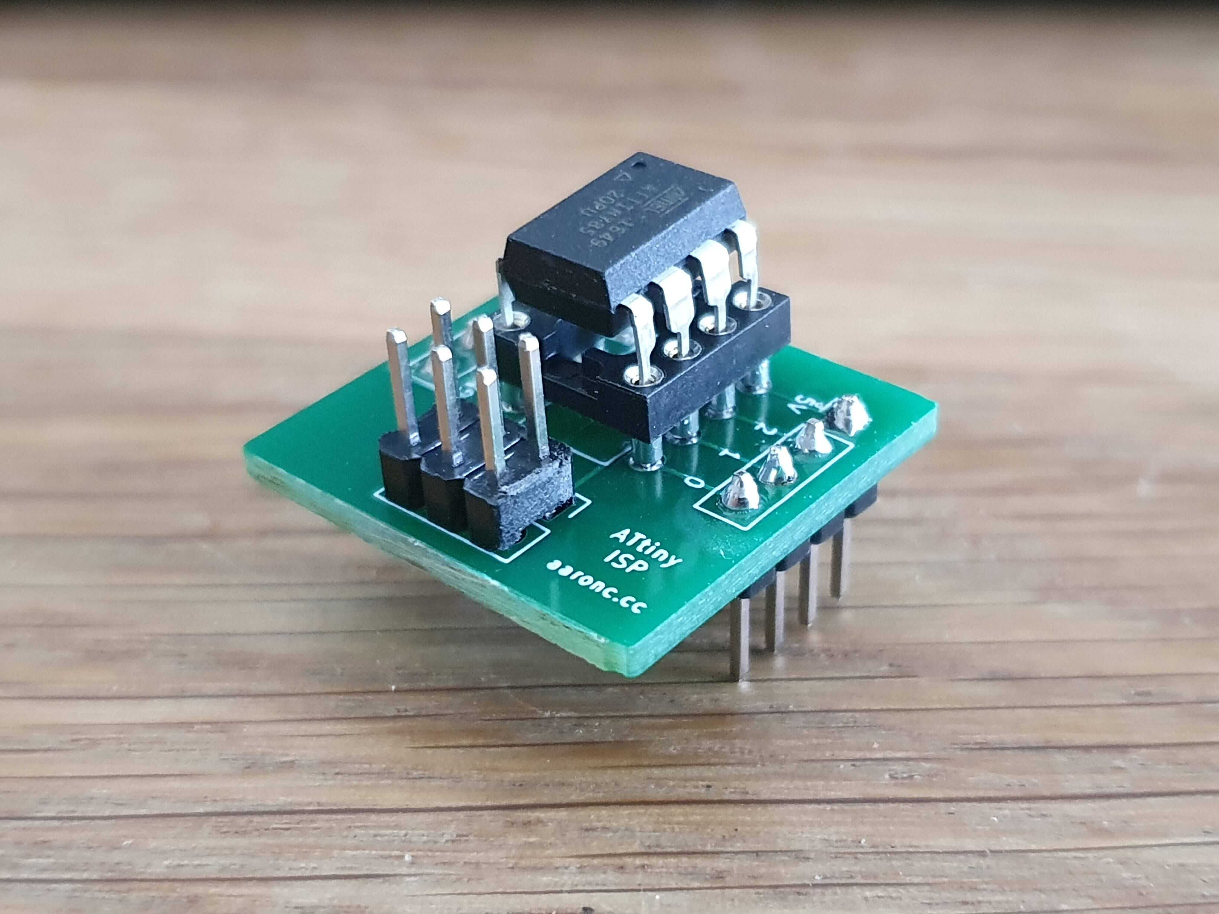
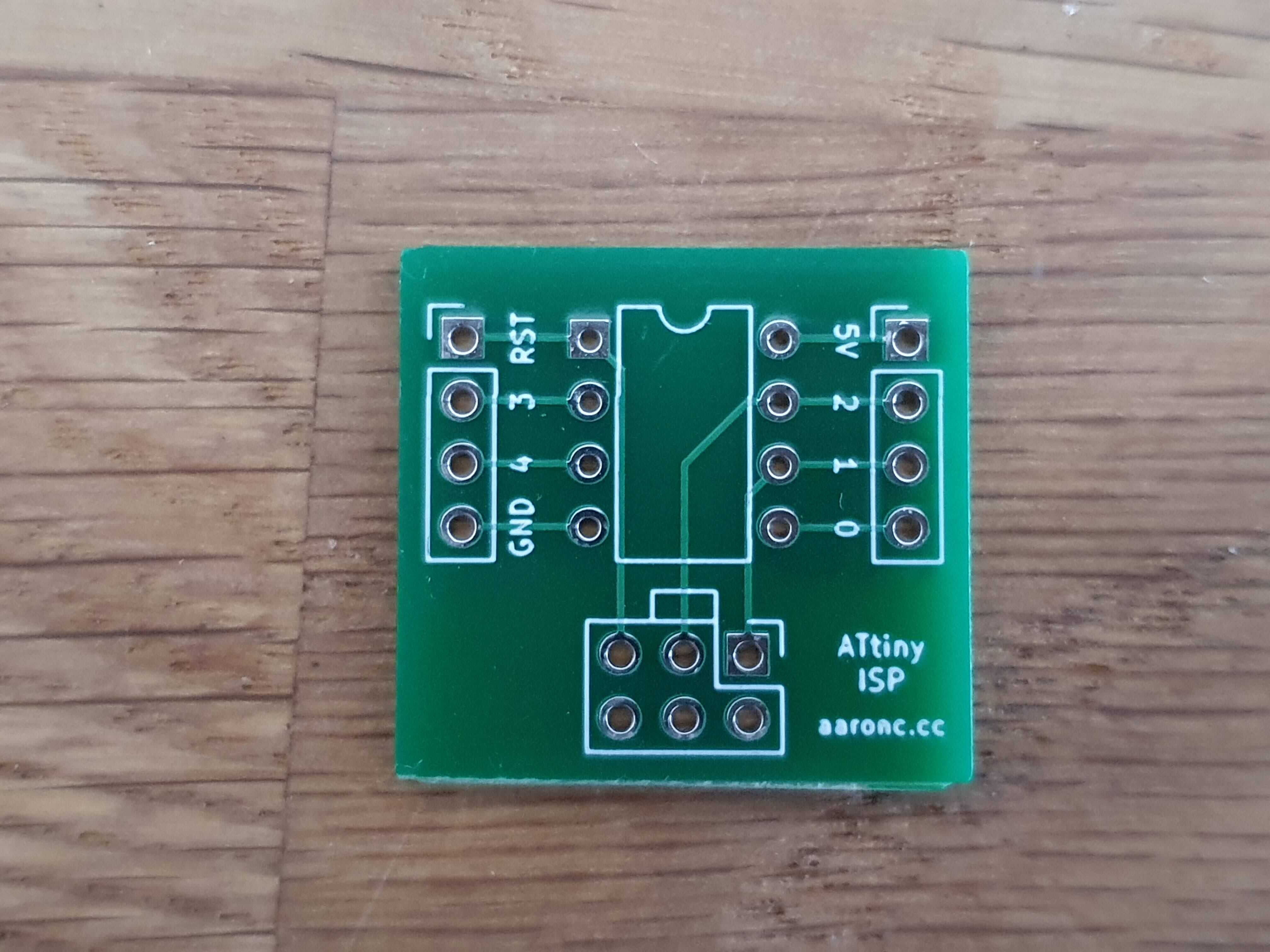
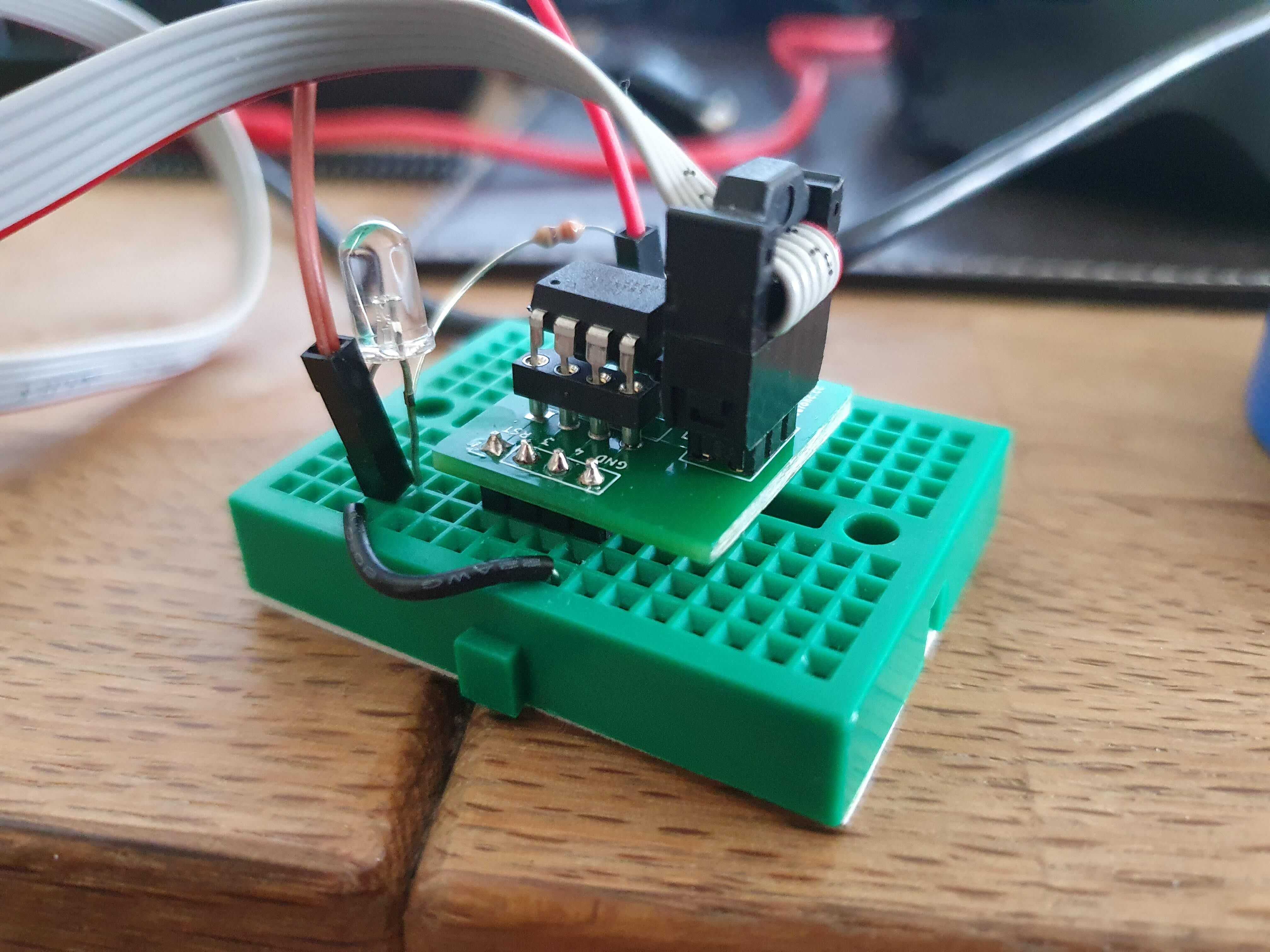
(I got mine fabricated by JLC, which worked out at about £5.50 for five boards, including delivery.)
It has a 6-pin ISP header for programming, so you'll need an AVR programmer. It also passes the ATtiny's pins through headers on the bottom of the board; this means you can plug it straight into a breadboard, and once you're done programming your ATtiny, simply remove the breakout and replace it with the lone chip.
It's been tested with an ATtiny85 (but should work on 25 and 45 too) and a Pololu USB AVR Programmer.
This repo contains all the KiCad files you should need. Open up the project in KiCad and build gerbers as required for your fabricator of choice!
| Qty | Value | Footprint | References |
|---|---|---|---|
| 1 | ATtiny85-20PU | Package_DIP:DIP-8_W7.62mm | U1 |
| 1 | AVR-ISP-6 | Connector_PinHeader_2.54mm:PinHeader_2x03_P2.54mm_Vertical | J3 |
| 1 | LeftConn | attiny85-breakout:PinHeader_1x04_P2.54mm_Vertical_FlippedModel | J1 |
| 1 | RightConn | attiny85-breakout:PinHeader_1x04_P2.54mm_Vertical_FlippedModel | J2 |
It measures 22.9 × 21.6 mm and has 2 copper layers, 1.6 mm thick.
4 parts, built around the ATTINY85-20PU. The full list of its parts is on this page, with links to each part's symbol and footprint where PCBKit's library has them.
From the AaronC81/attiny-breakout repository on GitHub, at the commit this page was made from: the board is attiny85-breakout.kicad_pcb. PCBKit opens the board in the browser, with nothing to install.
Its repository states no licence, so its author keeps all rights: ask AaronC81 before reusing the design.
bwack/C64-Switchless-Multi-Kernal-27C256-adapter
Kernal switcher for the C64/C64C/C128

plusvic/simplebus2-intercom
General description of the Simplebus2 protocol used by some Comelit's intercoms. Hardware for retransmitting Simplebus2 messages over UART.

osmocom/osmocom-analog
Software Implementation of analog cellular telephony systems like NMT, TACS, IMTS, A/B/C-Netz; mirror of https://gitea.osmocom.org/cellular-infrastructure/osmocom-analog

strickyak/jerboa-attiny85-mod-synth
Modular Synthesizer using an ATtiny85 chip for each module.


Hack-a-Day/Remoticon_KiCad_Blender
support files for the 2020 Remoticon KiCad to Blender > PCB renders workshop
