
6 layers235 × 225 mm
Dogrudan sdr A
kocer/direct-sampling-sdr
Direct-sampling SDR transceiver with four phase-coherent channels, and a class-A power amplifier for 1.8 to 54 MHz.
297 parts1
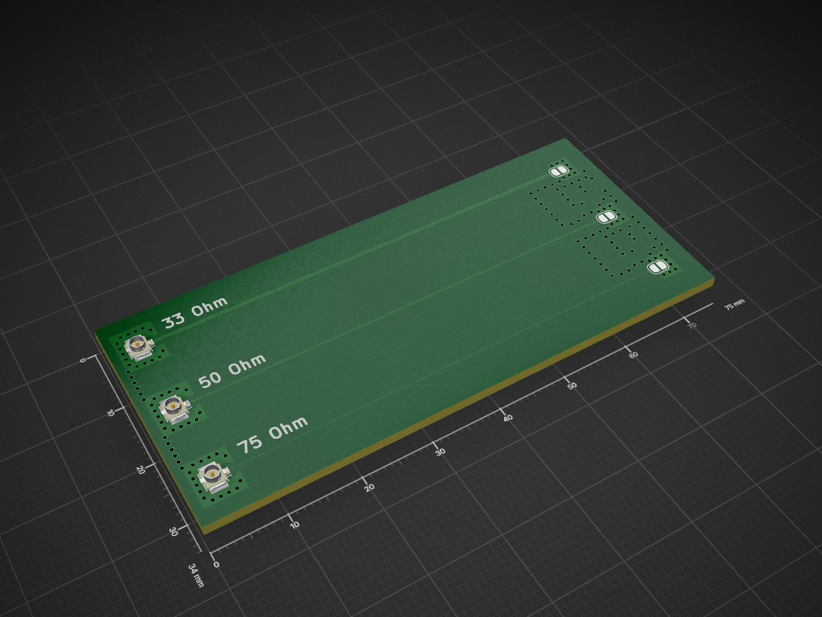
 TopQuark12/transmissionLineTest
PCB for testing nanoVNA's ability to measure impedance of PCB transmission line
TransmissionLineTest is an open-source printed circuit board by TopQuark12, from the TopQuark12/transmissionLineTest repository on GitHub. It is a 4-layer board of 75 × 34 mm with 14 parts on 12 nets, routed with 25 tracks and 154 vias.
It is built around the ADT1-1WT+.
| Qty | Value | Footprint | References |
|---|---|---|---|
| 7 | Jumper_NO_Small | Jumper:SolderJumper-2_P1.3mm_Open_RoundedPad1.0x1.5mm | JP1, JP2, JP3, JP6, JP7, JP8, JP9 |
| 5 | U.FL | Connector_Coaxial:U.FL_Hirose_U.FL-R-SMT-1_Vertical | J1, J2, J3, J4, J5 |
| 2 | ADT1-1WT+ | RF_Mini-Circuits:Mini-Circuits_CD542_H2.84mm | TR1, TR2 |
kocer/direct-sampling-sdr
Direct-sampling SDR transceiver with four phase-coherent channels, and a class-A power amplifier for 1.8 to 54 MHz.

StuckAtPrototype/Racer
These are structured into their own files. I could have used submodules, but decided against it.

hackclub/OnBoard
💡 Join 1,000 teenagers and make your first PCB with a $100 grant!

MicroCoreLabs/Projects
Ted Fried's MicroCore Labs Projects - FPGA CPU cores and emulators for the 8088, 8086, 8051, 6502, 68000, Z80, Risc-V, and also Typewriter and EPROM Emulator projects.


nanographs/Open-Beam-Interface
Just what you need to control the beam and get an image.

CRImier/MyKiCad
My KiCad boards. Can't be bothered uploading individually anymore, so here you go.

It measures 75 × 34 mm and has 4 copper layers, 1.6 mm thick.
14 parts, built around the ADT1-1WT+. The full list of its parts is on this page, with links to each part's symbol and footprint where PCBKit's library has them.
From the TopQuark12/transmissionLineTest repository on GitHub, at the commit this page was made from: the board is transmissionLineTest.kicad_pcb. PCBKit opens the board in the browser, with nothing to install.
Its repository states no licence, so its author keeps all rights: ask TopQuark12 before reusing the design.