
2 layers50 × 50 mm
Attiny44-ring
TheBeachLab/alphabets
Open Source Mechanical Split Flap Display, AKA Solari display
21 parts134MIT
 TheBeachLab/alphabets134
Open Source Mechanical Split Flap Display, AKA Solari display
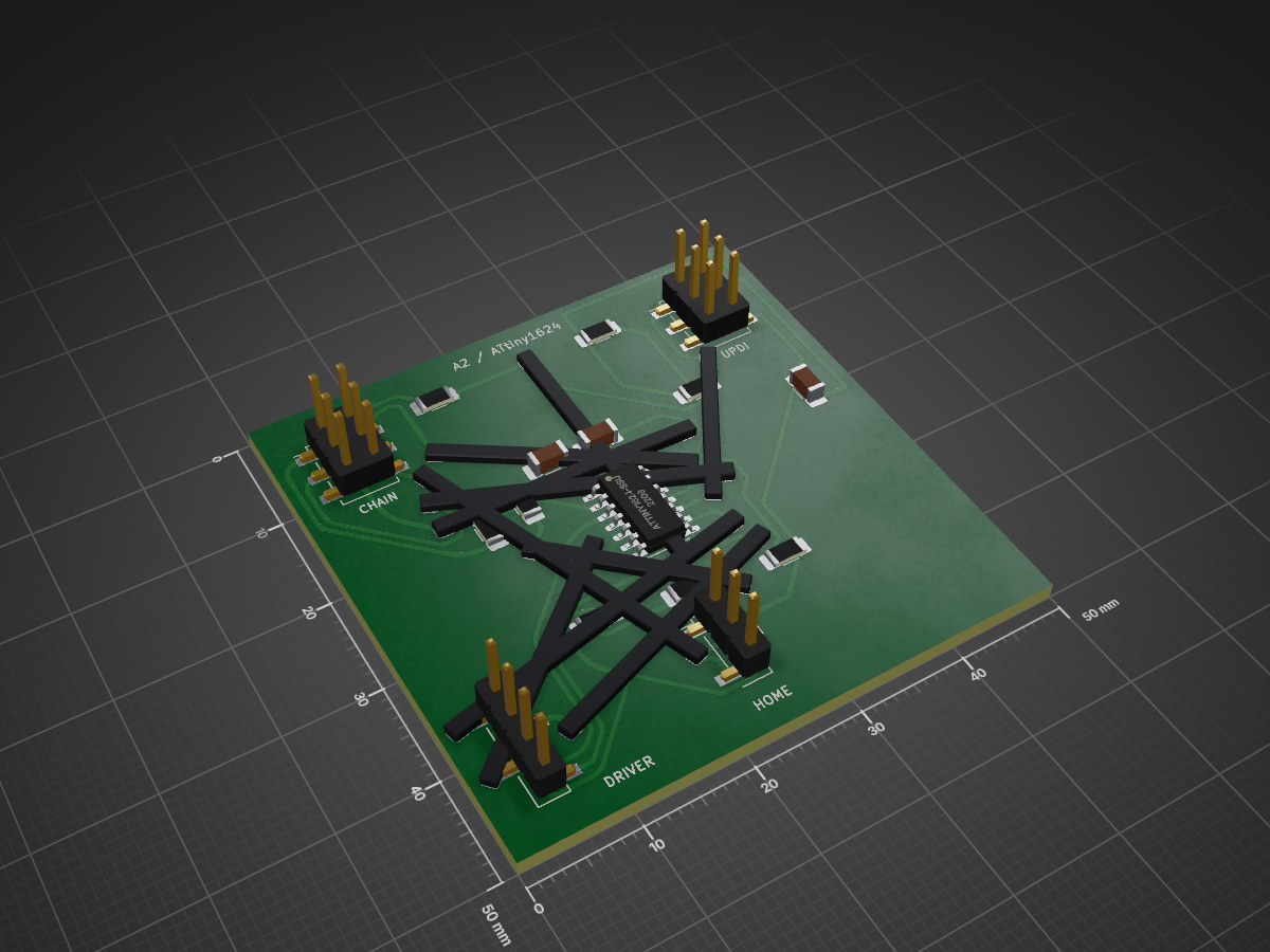
Attiny1624-ring is an open-source printed circuit board by TheBeachLab, from the TheBeachLab/alphabets repository on GitHub, published under the MIT licence. It is a 2-layer board of 50 × 50 mm with 26 parts on 33 nets, routed with 152 tracks and 0 vias.
It is built around the ATTINY1624-SSU. Its parts include 4 connectors, 3 capacitors, 2 resistors and 1 IC. It belongs with the lEDs and displays boards and the AVR (ATmega, ATtiny) boards of this library.
This directory contains the editable KiCad 10 design for one Alphabets V2 split-flap module. The board keeps the existing 2x3 synchronous-ring connector, drives an external four-input stepper board, reads a powered HOME sensor, and uses the ATtiny1624's one-wire UPDI programming interface.
The hardware assignment follows Microchip's ATtiny1624/1626/1627 data sheet. Microchip documents PA0 as UPDI/RESET and PA1, PA2, and PA3 as SPI0 MOSI, MISO, and SCK respectively. The standard programming connection is the 2x3, 2.54 mm UPDI header described in Microchip's UPDI connection guide.
U1: ATtiny1624-SSU in SOIC-14.J1: 2x3 SMD ring connector for LATCH, CLOCK, serial data, +5 V, and GND.J3: four logic outputs for the external stepper driver.J4: powered three-pin HOME sensor connector with a 10 kOhm pull-up.J5: 2x3 SMD UPDI connector; pins 1, 2, and 6 carry UPDI, target VDD, and
GND. Pins 3 through 5 are intentionally not connected.R1: 10 kOhm UPDI pull-up; R2: 10 kOhm HOME pull-up.C1: 100 nF local MCU decoupling; C2: 1 nF high-frequency bypass;
C3: 10 uF board bulk capacitance.JP1 through JP4, JP6, and JP9: removable 0 Ohm 1206
links that partition power, ground, and ring signals for assembly and
diagnosis.The board defines this ATtiny1624 signal assignment:
| Function | MCU signal | Physical pin |
|---|---|---|
| VDD | VDD | 1 |
| LATCH | PA4 / SPI0 SS | 2 |
| HOME | PA5 | 3 |
| Motor 4 | PB3 | 6 |
| Motor 3 | PB2 | 7 |
| Motor 2 | PB1 | 8 |
| Motor 1 | PB0 | 9 |
| UPDI | PA0 / UPDI | 10 |
| DATA_IN | PA1 / SPI0 MOSI | 11 |
| DATA_OUT | PA2 / SPI0 MISO | 12 |
| CLOCK | PA3 / SPI0 SCK | 13 |
| GND | GND | 14 |
PA6 and PA7 remain available and are intentionally not connected in this
revision. The matching firmware and host-side protocol tests are in
ATtiny1624 module firmware.
| Connector | Pinout |
|---|---|
J1 CHAIN | 1 LATCH, 2 CLOCK, 3 DATA_IN, 4 +5V, 5 DATA_OUT, 6 GND |
J3 DRIVER | 1 MOTOR1, 2 MOTOR2, 3 MOTOR3, 4 MOTOR4 |
J4 HOME | 1 +5V, 2 HOME, 3 GND |
J5 UPDI | 1 UPDI, 2 target VDD, 3-5 NC, 6 GND |
The chain connector follows the module protocol: pins 1, 2, 4, and 6 are bused, while pin 5 of one module feeds pin 3 of the next module.
F.Cu; the design contains no vias or back-copper
tracks.Ten insulated wire links cross above the routed copper. Solder insulated wire
between the two pads of each footprint; the dashed F.Fab line marks its
assembly path and is not copper:
| Reference | Signal | Pad spacing |
|---|---|---|
JP5 | CLOCK | 22.3 mm |
JP7 | DATA_IN | 25.6 mm |
JP8 | DATA_OUT | 23.5 mm |
JP10 | UPDI | 16.6 mm |
JP11 | chain GND | 29.7 mm |
JP12 | motor phase 3 | 23.5 mm |
JP13 | MCU power source | 17.7 mm |
JP14 | motor phase 1 | 30.3 mm |
JP15 | motor phase 2 | 24.5 mm |
JP16 | main power distribution | 27.0 mm |
attiny1624-ring.kicad_pro, .kicad_sch, and .kicad_pcb: editable
native KiCad project files.fabrication/: Gerbers, drill outputs, BOM, positions, and STEP model.preview/: top render, front-copper drawing, and schematic drawing.validation/: ERC and DRC/schematic-parity reports.routing/attiny1624-ring.ses: checked-in single-layer routing session.tools/: deterministic generators, route import, organic post-processing,
and project-specific electrical/mechanical checks.The normal reproducible path starts from the checked-in route:
make schematic board route organic check fabrication previewsSet KICAD_CLI, KICAD_PYTHON, KIUTILS_PYTHON, and
KICAD10_FOOTPRINT_DIR for the installed KiCad environment. When placement or
the netlist changes, create a new session with:
make autoroute FREEROUTING_JAR=/path/to/freerouting.jarmake check enforces the 50 x 50 mm outline, front-copper-only routing, zero
vias, 16/20 mil widths, ten wire links, native arcs, teardrops, zero ERC/DRC
violations, zero unrouted connections, and exact schematic-to-PCB parity.
| Qty | Value | Footprint | References |
|---|---|---|---|
| 1 | 0R CHAIN power bridge 1206 | Resistor_SMD:R_1206_3216Metric_Pad1.30x1.75mm_HandSolder | JP1 |
| 1 | 0R HOME power bridge 1206 | Resistor_SMD:R_1206_3216Metric_Pad1.30x1.75mm_HandSolder | JP3 |
| 1 | 0R LATCH bridge 1206 | Resistor_SMD:R_1206_3216Metric_Pad1.30x1.75mm_HandSolder | JP6 |
| 1 | 0R MCU ground bridge 1206 | Resistor_SMD:R_1206_3216Metric_Pad1.30x1.75mm_HandSolder | JP9 |
| 1 | 0R MCU power bridge 1206 | Resistor_SMD:R_1206_3216Metric_Pad1.30x1.75mm_HandSolder | JP4 |
| 1 | 0R UPDI power bridge 1206 | Resistor_SMD:R_1206_3216Metric_Pad1.30x1.75mm_HandSolder | JP2 |
| 1 | 100n MCU 1206 | Capacitor_SMD:C_1206_3216Metric_Pad1.33x1.80mm_HandSolder | C1 |
| 1 | 10k HOME pull-up 1206 | Resistor_SMD:R_1206_3216Metric_Pad1.30x1.75mm_HandSolder | R2 |
| 1 | 10k UPDI pull-up 1206 | Resistor_SMD:R_1206_3216Metric_Pad1.30x1.75mm_HandSolder | R1 |
| 1 | 10u BULK 1206 | Capacitor_SMD:C_1206_3216Metric_Pad1.33x1.80mm_HandSolder | C3 |
| 1 | 1n HF 1206 | Capacitor_SMD:C_1206_3216Metric_Pad1.33x1.80mm_HandSolder | C2 |
| 1 | ATtiny1624-SSU | Package_SO:SOIC-14_3.9x8.7mm_P1.27mm | U1 |
| 1 | CHAIN_RING | Connector_PinHeader_2.54mm:PinHeader_2x03_P2.54mm_Vertical_SMD | J1 |
| 1 | HOME_SENSOR | Connector_PinHeader_2.54mm:PinHeader_1x03_P2.54mm_Vertical_SMD_Pin1Left | J4 |
| 1 | INSULATED CLOCK LINK 22.3mm | Alphabets:WireLink_22.3mm_SMD | JP5 |
| 1 | INSULATED DATA_IN LINK 25.6mm | Alphabets:WireLink_25.6mm_SMD | JP7 |
| 1 | INSULATED DATA_OUT LINK 23.5mm | Alphabets:WireLink_23.5mm_SMD | JP8 |
| 1 | INSULATED GND LINK 29.7mm | Alphabets:WireLink_29.7mm_SMD | JP11 |
| 1 | INSULATED MAIN POWER LINK 27.0mm | Alphabets:WireLink_27.0mm_SMD | JP16 |
| 1 | INSULATED MCU POWER LINK 17.7mm | Alphabets:WireLink_17.7mm_SMD | JP13 |
| 1 | INSULATED MOTOR1 LINK 30.3mm | Alphabets:WireLink_30.3mm_SMD | JP14 |
| 1 | INSULATED MOTOR2 LINK 24.5mm | Alphabets:WireLink_24.5mm_SMD | JP15 |
| 1 | INSULATED MOTOR3 LINK 23.5mm | Alphabets:WireLink_23.5mm_SMD | JP12 |
| 1 | INSULATED UPDI LINK 16.6mm | Alphabets:WireLink_16.6mm_SMD | JP10 |
| 1 | STEPPER_DRIVER_IN | Connector_PinHeader_2.54mm:PinHeader_1x04_P2.54mm_Vertical_SMD_Pin1Left | J3 |
| 1 | UPDI_2X3 | Connector_PinHeader_2.54mm:PinHeader_2x03_P2.54mm_Vertical_SMD | J5 |
TheBeachLab/alphabets
Open Source Mechanical Split Flap Display, AKA Solari display

KrystianD/avr-power-meter
AVR-based, galvanically isolated, bidirectional DC energy meter with Modbus RTU interface.

matty337s/Webasto-Heater-WBUS-Controller
Controller for webasto heater used in vehicles such as Land Rover Discovery 3. Used to turn on and off heater using ATTINY microcontroller, with inputs for USB, ignition and low-beam.


lepi-labs/1-synth-badge
ATTINY1624 powered PCB badge with light up eyes and horns

NerdFlare/NF-SolderChallenge27
Art, code, and pcb for the AY26-27 NF, IEEE, CPES solder challenge!

penayush-tronics/ATtinyStep
An ATtiny powered step counter and speed/distance measuring device that fits in the palm of your hand.


It measures 50 × 50 mm and has 2 copper layers, 1.6 mm thick.
26 parts, built around the ATTINY1624-SSU. The full list of its parts is on this page, with links to each part's symbol and footprint where PCBKit's library has them.
From the TheBeachLab/alphabets repository on GitHub, at the commit this page was made from: the board is V2/Hardware/Final/electronics/attiny1624-ring/attiny1624-ring.kicad_pcb and its schematic V2/Hardware/Final/electronics/attiny1624-ring/attiny1624-ring.kicad_sch. PCBKit opens the board in the browser, with nothing to install.
Its repository publishes it under the MIT licence: you may reuse it on that licence's terms (keep the author's notice, and for a copyleft licence share your changes alike).