2 layers100 × 100 mm
 That-Canadian/Keyboard_Files13
My open source keyboard files will go here
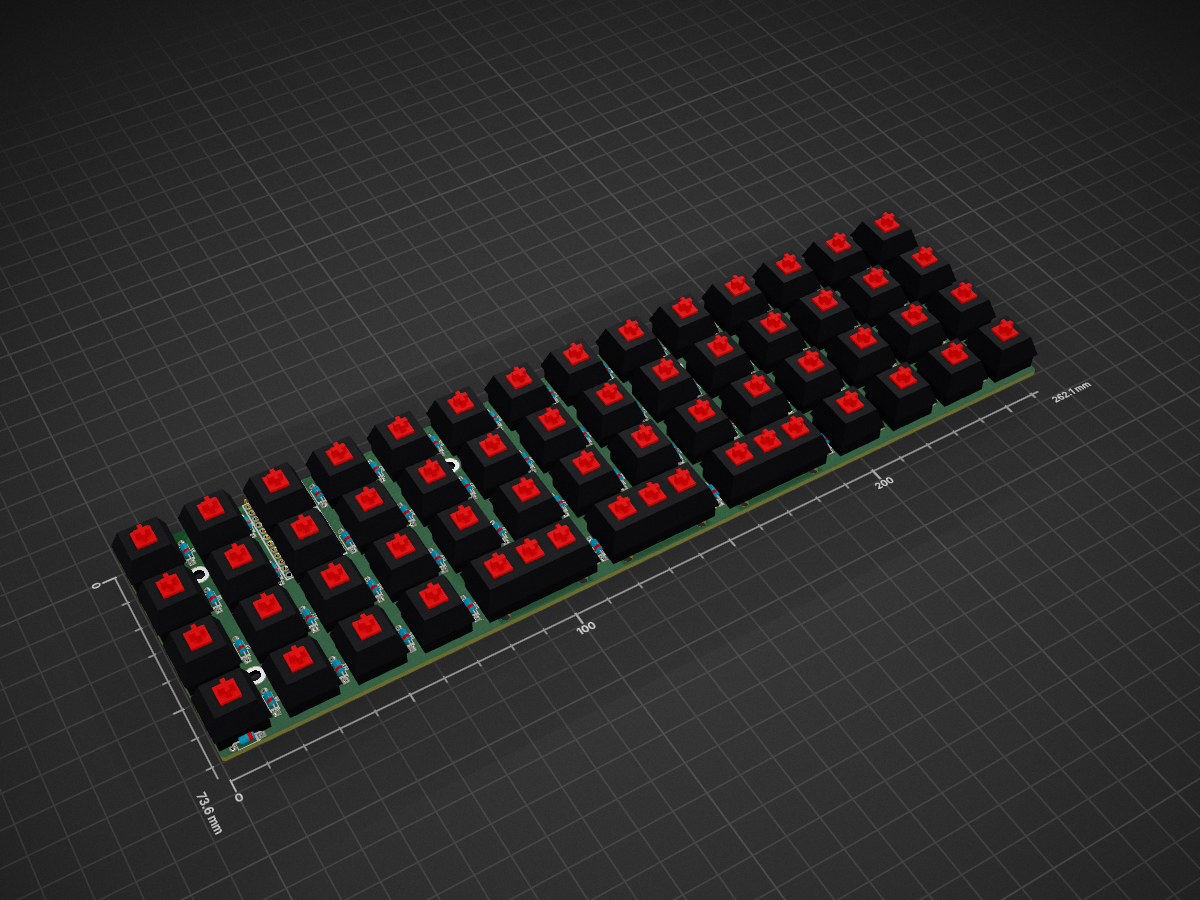
Eco Board is an open-source printed circuit board by That-Canadian, from the That-Canadian/Keyboard_Files repository on GitHub. It is a 2-layer board of 262.1 × 73.6 mm with 129 parts on 78 nets, routed with 539 tracks and 15 vias.
Its parts include 59 switches, 56 diodes and 1 IC. It belongs with the keyboards and input boards and the AVR (ATmega, ATtiny) boards of this library.
My Open Source keyboard files will be places here.
-- TODO: Better README --
| Qty | Value | Footprint | References |
|---|---|---|---|
| 56 | D | canadian_footprints:D_SOD123_ThroughHole | D1, D2, D10, D11, D12, D13, D14, D15, D16, D17, D18, D19, D20, D21, D22, D23 +40 |
| 56 | SW_PUSH | canadian_footprints:Mx_Alps_100 | SW1, SW2, SW10, SW11, SW12, SW13, SW14, SW15, SW16, SW17, SW18, SW19, SW21, SW22, SW23, SW24 +40 |
| 1 | LOGO | canadian_footprints:maple-8mm | G*** |
| 1 | LOGO | bishop-logos:BKB smaller chess | G*** |
| 1 | LOGO | eco:eco | G*** |
| 1 | ProMicro | canadian_footprints:Pro_Micro | U1 |
| 1 | SW_PUSH | canadian_footprints:SW_TACT_ALPS_SKQGABE010 | RESET1 |
| 1 | sw_dbl1 | canadian_footprints:Mx_Alps_200 | SW20 |
| 1 | sw_dbl2 | canadian_footprints:Mx_Alps_200 | SW29 |
| 1 | sw_dbl3 | canadian_footprints:Mx_Alps_200 | SW38 |
The 120 most common of 129 parts.


jackw01/pi-tin
Open source raspberry pi handheld retro gaming console

BathroomEpiphanies/KiCAD-Keyboard-Tutorial
Tutorial on making keyboard PCB layouts in KiCAD


It measures 262.1 × 73.6 mm and has 2 copper layers, 1.6 mm thick.
129 parts. The full list of its parts is on this page, with links to each part's symbol and footprint where PCBKit's library has them.
From the That-Canadian/Keyboard_Files repository on GitHub, at the commit this page was made from: the board is ECO Keyboard/PCB Files/V2.1/Eco-Board.kicad_pcb. PCBKit opens the board in the browser, with nothing to install.
Its repository states no licence, so its author keeps all rights: ask That-Canadian before reusing the design.