

2 layers52.2 × 52.2 mm
Base
google/mozc-devices
Circuit diagrams and firmware source code for Gboard DIY keyboards
43 parts3kApache-2.0

PCB converion of the HAGIWO envelope follower module.
Main pcb v2 is an open-source printed circuit board by Testbild-synth, from the Testbild-synth/Hagiwo_043_envelope_follower repository on GitHub. It is a 2-layer board of 29 × 85 mm with 43 parts on 35 nets, routed with 342 tracks and 15 vias.
It is built around the TL072IPE4. Its parts include 19 resistors, 9 capacitors, 4 diodes, 3 connectors and 2 ICs.
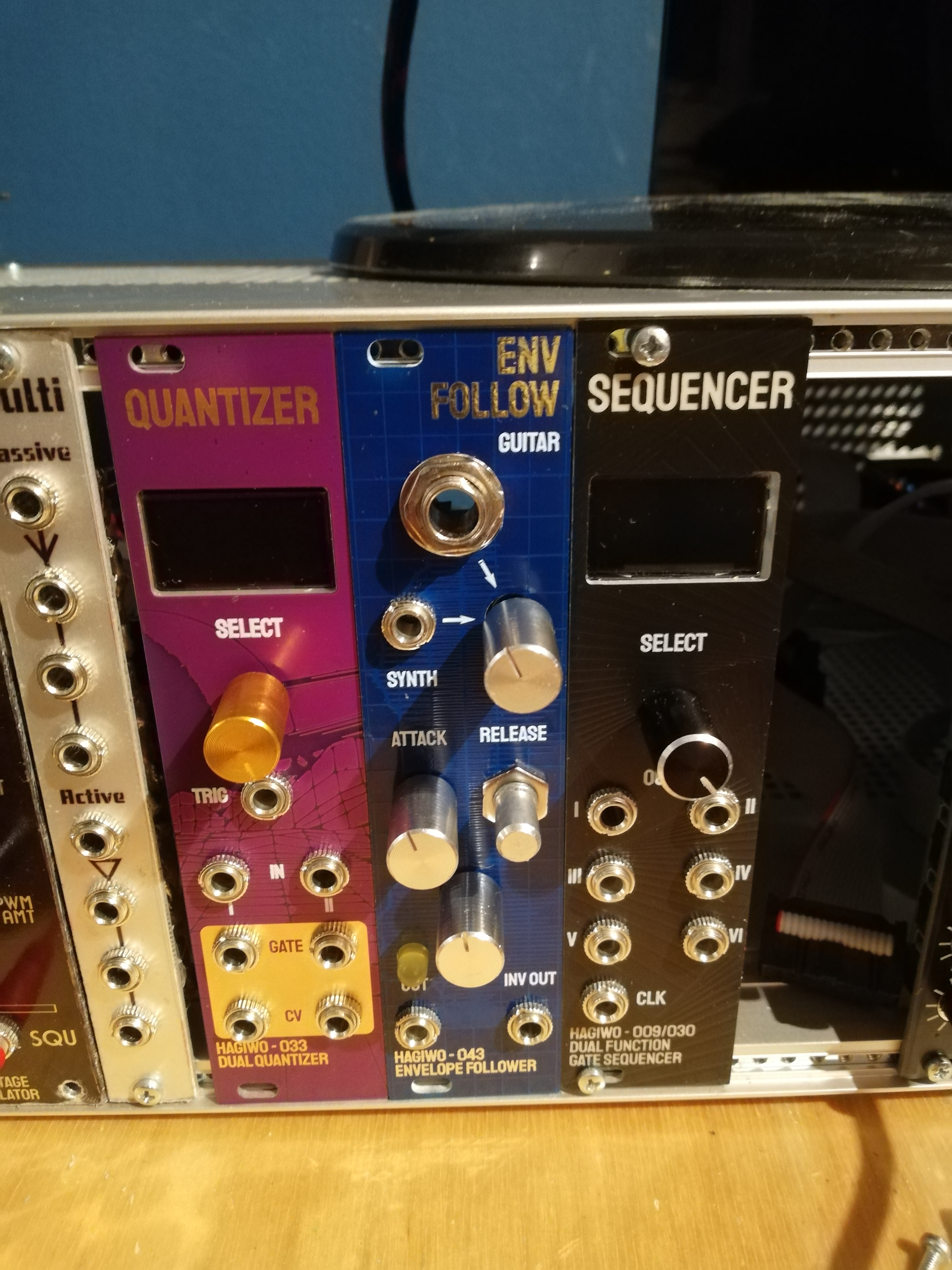
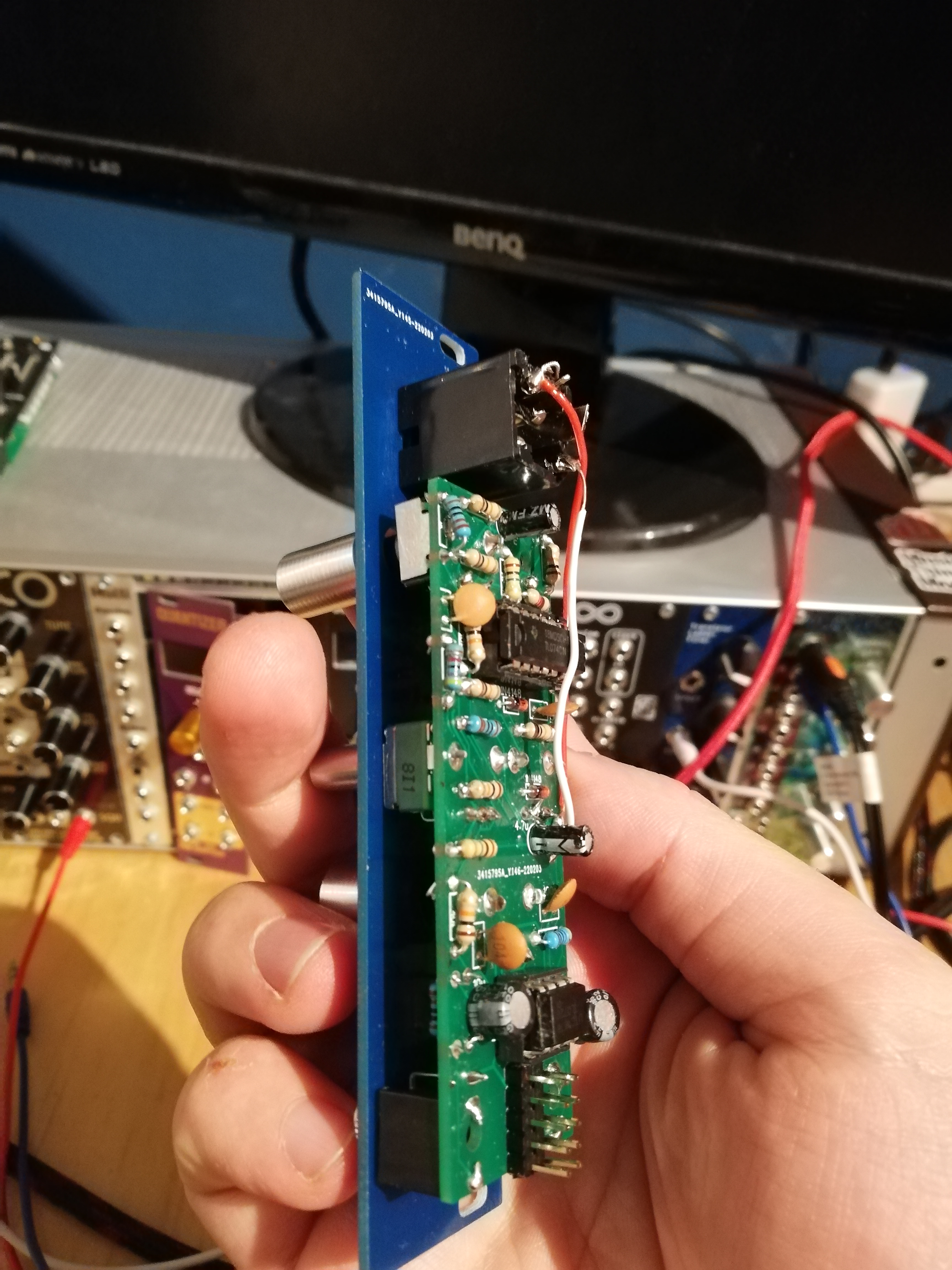
This project is a through hole PCB version the HAGIWO 043 envelope follower. I also added a guitar jack input with more amplification to be able to plug in a variety of instruments.
For this one I wanted to fit it all onto one PCB and make the guitar jack fit. This was quite a task and I'm afraid the pcb ended up a bit messy in the end because of this. It still works fine, but has a lot of overlapping components and you have to be careful when building it.
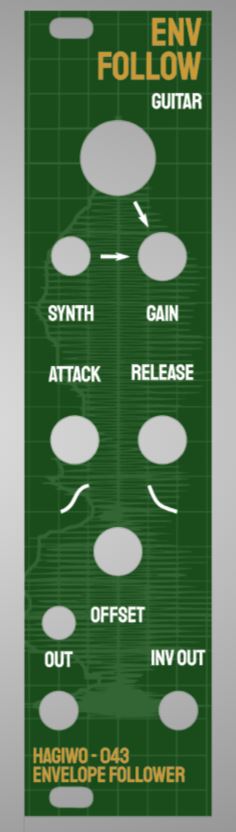
You can find the schematic and BOM in the root folder. For the PCBs, the module has one circuit PCB and one panel PCB. You can order them on any common PCB manufacturing service, I used JLCPCB. For the circuit PCB, standard settings should be fine. For the panel, since it has copper exposed, make sure to choose a lead free surface finish (LeadFree HASL, ENIG) and/or spraypaint your panels so that you don't get lead on your hands.
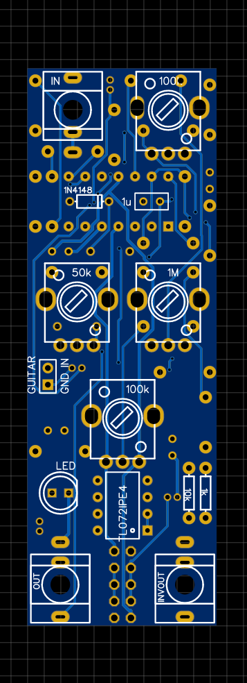
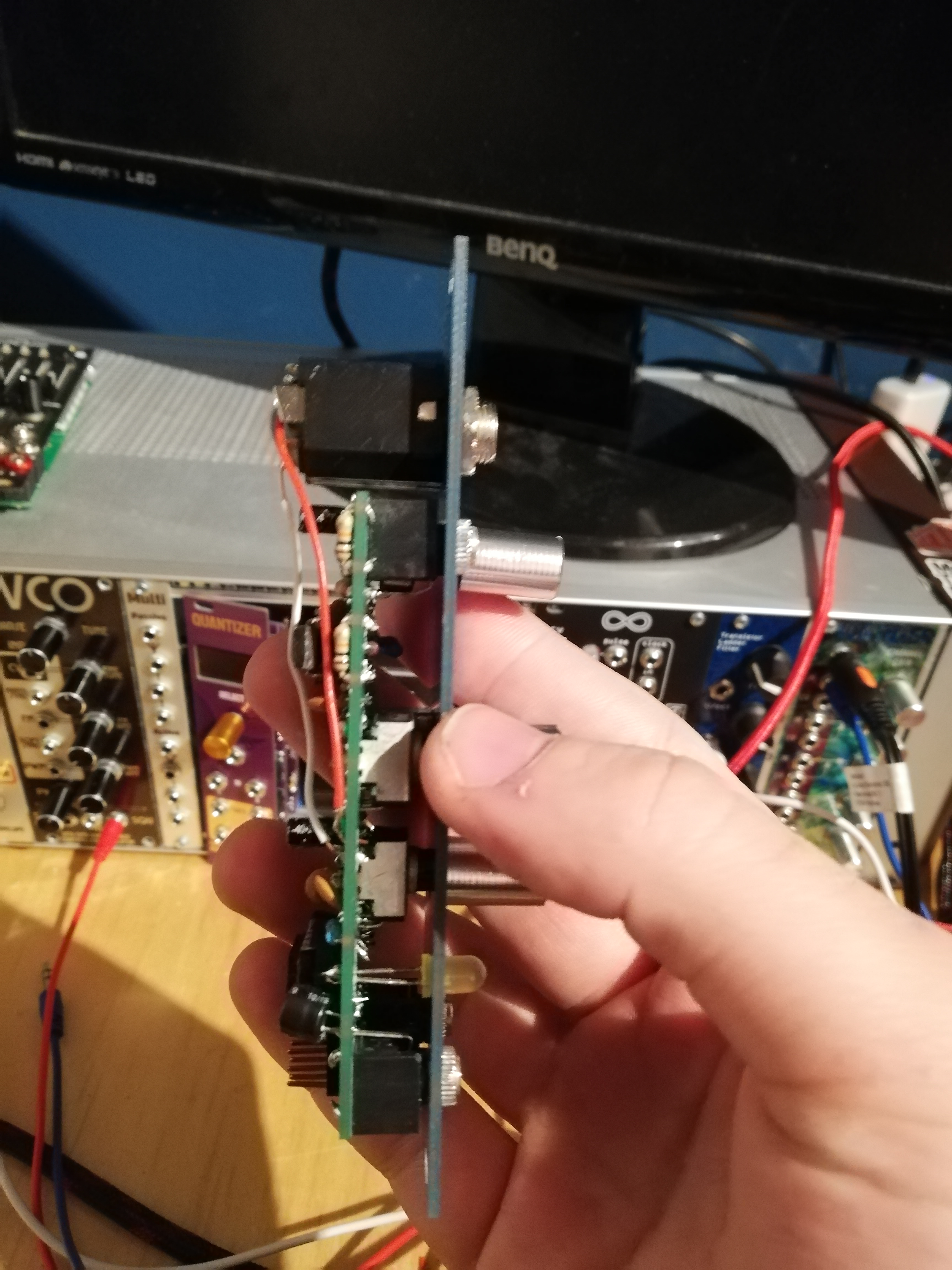
For assembly, the guitar jack is optional. It will stick out and has to be connected to the rest of the pcb via wires. Look for the pads named "guitar in" and "gnd" on the pcb and connect those to the inner and outer log of a mono guitar/6.5mm jack socket. Be sure to get a pcb mount guitar jack! we will not be mounting it to the pcb but the "normal" round ones don't fit the spacing. I got this!
| Qty | Value | Footprint | References |
|---|---|---|---|
| 9 | 10k | easyeda:R_AXIAL-0.3 | R3, R7, R8, R9, R13, R14, R15, R16, R17 |
| 4 | 100n | easyeda:RAD-0.1 | C4, C6, C8, C9 |
| 3 | 1k | easyeda:R_AXIAL-0.3 | R5, R12, R18 |
| 3 | DIODE1N4148 | easyeda:SEEED-DO-35 | D1, D2, D3 |
| 2 | 100k | easyeda:R09-5KΩ | GAIN, OFFSET |
| 2 | 10u | easyeda:CAP-D4.0×F1.5 | C5, C7 |
| 2 | 1M | easyeda:R_AXIAL-0.3 | R6, R11 |
| 2 | 4.7k | easyeda:R_AXIAL-0.3 | R10, R19 |
| 2 | 4.7u | easyeda:CAP-D4.0×F1.5 | C1, C3 |
| 1 | 1M | easyeda:R09-5KΩ | REL |
| 1 | 1u | easyeda:RAD-0.1 | C2 |
| 1 | 20k | easyeda:R_AXIAL-0.3 | R1 |
| 1 | 22k | easyeda:R_AXIAL-0.3 | R2 |
| 1 | 47k | easyeda:R_AXIAL-0.3 | R4 |
| 1 | 50k | easyeda:R09-5KΩ | ATK |
| 1 | EURORACK_POWERHEADER_V2 | easyeda:EURORACK_POWER_V2 | EP1 |
| 1 | GUITAR | easyeda:HDR-F-2.54_1X2 | H1 |
| 1 | IN | easyeda:THONKICONN_1 | J1 |
| 1 | INVOUT | easyeda:THONKICONN_1 | J3 |
| 1 | LED_LED5MM | easyeda:LED_LED5MM | LED1 |
| 1 | OUT | easyeda:THONKICONN_1 | J2 |
| 1 | TL072IPE4 | easyeda:DIP8 | U2 |
| 1 | TL074CJ | easyeda:DIP14 | U1 |
google/mozc-devices
Circuit diagrams and firmware source code for Gboard DIY keyboards

rusefi/rusefi
rusefi - GPL internal combustion engine control unit


jrsteensen/OpenHornet
OpenHornet 1:1 F/A-18C Simulator Repository


tebl/RC6502-Apple-1-Replica
An expandable SBC-version of the Apple 1 computer, easy to get started with and lot of cool stuff that can be added to it!

nodestark/mdb-esp32-cashless
ESP32-based MDB cashless device for vending machines, supporting EVA DTS DEX/DDCMP telemetry and payments over the MDB protocol via Bluetooth and MQTT

zynthian/zynthian-hw
Zynthian hardware stuff: PCBs, schemes, parts specifications, pin assignment, ...
It measures 29 × 85 mm and has 2 copper layers.
43 parts, built around the TL072IPE4. The full list of its parts is on this page, with links to each part's symbol and footprint where PCBKit's library has them.
From the Testbild-synth/Hagiwo_043_envelope_follower repository on GitHub, at the commit this page was made from: the board is design files/pcb/main_pcb_v2.kicad_pcb. PCBKit opens the board in the browser, with nothing to install.
Its repository states no licence, so its author keeps all rights: ask Testbild-synth before reusing the design.