
2 layers99.1 × 53.3 mm

VGA Breakout Board
D Sub-9 is an open-source printed circuit board by T-Pau, from the T-Pau/Connector-Breakout-Boards repository on GitHub. It is a 2-layer board of 81.3 × 53.3 mm with 3 parts on 14 nets, routed with 66 tracks and 0 vias.
They provide easy access to each pin of a connector via a pin header, labeled with the pin number and its use. If a connector contains multiple ground pins, these can be connected on the board via jumpers.
They make testing or prototyping cables easier by providing a robust connection and avoiding mixing up pins.
You can produce these boards
These connectors saw a wide variety of uses, therefore only pin numbers are provided on the silk screen. Each breakout board contains a pins and a socket connector.
| Amount | Part |
|---|---|
| 1 | 90° D-Sub-9 pins |
| 1 | 90° D-Sub-9 socket |
| 1 | 2x5 pin header |
| Amount | Part |
|---|---|
| 1 | 90° D-Sub-15 pins |
| 1 | 90° D-Sub-15 socket |
| 1 | 2x8 pin header |
| Amount | Part |
|---|---|
| 1 | 90° D-Sub-25 plug |
| 1 | 90° D-Sub-25 socket |
| 1 | 2x13 pin header |
This board exposes each pin of a VGA connector on a pin header. It also allows connecting each of the GND pins via jumpers.
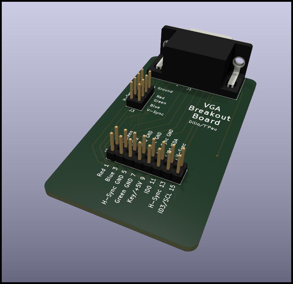
| Amount | Part |
|---|---|
| 1 | 90° D-Sub-15 HD socket |
| 1 | 2x4 pin header |
| 1 | 2x8 pin header |
| 4 | jumper |
| Qty | Value | Footprint | References |
|---|---|---|---|
| 1 | Breakout | Connector_PinHeader_2.54mm:PinHeader_2x05_P2.54mm_Vertical | J3 |
| 1 | Pins | Connector_Dsub:DSUB-9_Pins_Horizontal_P2.77x2.84mm_EdgePinOffset7.70mm_Housed_MountingHolesOffset9.12mm | J1 |
| 1 | Socket | Connector_Dsub:DSUB-9_Socket_Horizontal_P2.77x2.84mm_EdgePinOffset7.70mm_Housed_MountingHolesOffset9.12mm | J2 |


hzeller/rpi-rgb-led-matrix
Controlling up to three chains of 64x64, 32x32, 16x32 or similar RGB LED displays using Raspberry Pi GPIO


atopile/atopile
Design circuit boards with code! ✨ Get software-like design reuse 🚀, validation, version control and collaboration in hardware; starting with electronics ⚡️


hackclub/sprig
🍃 Learn to code by making games in a JavaScript web-based game editor.
It measures 81.3 × 53.3 mm and has 2 copper layers, 1.6 mm thick.
3 parts. The full list of its parts is on this page, with links to each part's symbol and footprint where PCBKit's library has them.
From the T-Pau/Connector-Breakout-Boards repository on GitHub, at the commit this page was made from: the board is D-Sub-9/D-Sub-9.kicad_pcb and its schematic D-Sub-15/D-Sub-15.kicad_sch. PCBKit opens the board in the browser, with nothing to install.
Its repository states no licence, so its author keeps all rights: ask T-Pau before reusing the design.