

2 layers368.3 × 215.9 mm

 SukkoPera/Hannes5128
512 kB RAM Expansion for the Commodore 16/+4
Hannes512 is an open-source printed circuit board by SukkoPera, from the SukkoPera/Hannes512 repository on GitHub. It is a 2-layer board of 54.3 × 72.2 mm with 25 parts on 73 nets, routed with 801 tracks and 119 vias.
It is built around the 74HCT245, 74HCT02D and 74HCT573D, with the NE555 among its other parts. Its parts include 9 ICs, 7 capacitors, 3 connectors and 2 resistors. It belongs with the retro computing and games boards of this library.


Hannes512 is an Open Hardware internal 512 kB RAM Expansion board for the Commodore 16.
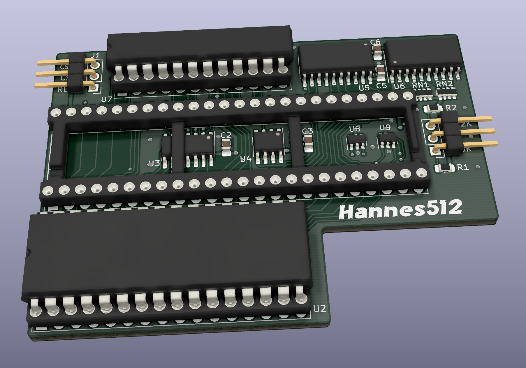
While making Hannes256 two shortcomings became apparent:
It was pretty obvious that switching to a modern SRAM would alleviate both issues, so I went looking for modern chips I could use and the Alliance AS6C4008 turned out to be a perfect match. Besides, it is 512 kB so I even went beyond the original goals and made all of that available to the C16 (even though that can create incompatibilities, see below).
This board is basically a variant of Hannes256, so most of what you can read on that page also applies to this board.
One exception is that I reintroduced the ESD protection diodes for the TED that were featured in Fixteen. They are U8 and U9 and they are optional.
Both AS6C4008-55PCN and -55PIN have been tested and work fine. I don't know about any other chips, but it's possible that other SRAMs will work.
AS6C4008 chips can either be bought new from electronic distributors or (probably-) used from AliExpress. I have bought a few of the latter and they were all working correctly.
See Hannes256.
While the mechanism originally devised by Hannes/Solder for 256 kB memory expansion can easily be extended to 512 kB and even 1 MB expansions, it requires that software programmers behave correctly and consider the default bank to be bank 15. Unfortunately, some of the software requiring 256 kB that already exists was written with the assumption that no expansion larger than 256 kB would ever surface and sets bits 2/3 of the expansion control register to 0 when wanting to switch to the default bank.
This problem affects Dream World and even the modern-era Lykia, for instance. The only real solution is to patch the software, but until someone does that, another option is to just limit memory expansions to 256 kB. After all, there is no software (... yet!) that needs more than that, so it currently looks like an acceptable compromise.
The great news is that this is rather easy to do in Hannes512, you just need to program the GAL with a different file. The gal directory contains a number of different JED files:
Feel free to open an issue if you have some suggestions on this topic.
See Hannes256.
See Hannes256, but keep in mind what is said in the Technical Notes above.
If you want to get this board produced, you are recommended to get the latest release rather than the current git version, as the latter might be under development and is not guaranteed to be working.
Every release is accompanied by its Bill Of Materials (BOM) file and any relevant notes about it, which you are recommended to read carefully.
The Hannes512 documentation, including the design itself, is copyright © SukkoPera 2022-2023 and is licensed under the Creative Commons Attribution-NonCommercial-ShareAlike 4.0 International License.
This documentation is distributed as is and WITHOUT ANY EXPRESS OR IMPLIED WARRANTIES whatsoever with respect to its functionality, operability or use, including, without limitation, any implied warranties OF MERCHANTABILITY, SATISFACTORY QUALITY, FITNESS FOR A PARTICULAR PURPOSE or infringement. We expressly disclaim any liability whatsoever for any direct, indirect, consequential, incidental or special damages, including, without limitation, lost revenues, lost profits, losses resulting from business interruption or loss of data, regardless of the form of action or legal theory under which the liability may be asserted, even if advised of the possibility or likelihood of such damages.
If you want to get some boards manufactured, you can get them from PCBWay through this link:

You get my gratitude and cheap, professionally-made and good quality PCBs, I get some credit that will help with this and other projects. You won't even have to worry about the various PCB options, it's all pre-configured for you!
Also, if you still have to register, you can use this link to get some bonus initial credit (and yield me some more).
You can also buy me a coffee if you want:

| Qty | Value | Footprint | References |
|---|---|---|---|
| 6 | 100n | Capacitor_SMD:C_0805_2012Metric_Pad1.18x1.45mm_HandSolder | C1, C2, C4, C5, C6, C7 |
| 2 | 10k | Resistor_SMD:R_0805_2012Metric_Pad1.20x1.40mm_HandSolder | R1, R2 |
| 2 | 1k | Resistor_SMD:R_Array_Convex_4x0603 | RN1, RN2 |
| 2 | DT1042 | Package_SO:TSOP-6_1.65x3.05mm_P0.95mm | U8, U9 |
| 1 | 10n | Capacitor_SMD:C_0805_2012Metric_Pad1.18x1.45mm_HandSolder | C3 |
| 1 | 74HCT02 | Package_SO:SOIC-14_3.9x8.7mm_P1.27mm | U3 |
| 1 | 74HCT245 | Package_SO:SO-20_5.3x12.6mm_P1.27mm | U6 |
| 1 | 74HCT573 | Package_SO:SO-20_5.3x12.6mm_P1.27mm | U5 |
| 1 | AS6C4008 | Package_DIP:DIP-32_W15.24mm_Socket_LongPads | U2 |
| 1 | CC_LOGO | Hannes512:cc_by_nc_sa | V1 |
| 1 | CONN_CS | Connector_PinHeader_2.54mm:PinHeader_1x03_P2.54mm_Vertical | J1 |
| 1 | GAL20V8 | Package_DIP:DIP-24_W7.62mm_Socket | U7 |
| 1 | LOGO | Hannes512:logo | V2 |
| 1 | MOS_7360_TED | Package_DIP:DIP-48_W15.24mm_Socket_LongPads | U1 |
| 1 | NE555 | Package_SO:SOIC-8_3.9x4.9mm_P1.27mm | U4 |
| 1 | RAM_SELECTOR | Connector_PinHeader_2.54mm:PinHeader_1x03_P2.54mm_Vertical | J2 |
| 1 | TED_SOCKET | Hannes512:DIP-48_W15.24mm_LongPads_ModSilkS | J0 |

ifilot/morseboard-8088
Single board computer designed around the 8088 processor


MicroLind-Developers/microlind-hw
Hardware repository for the microlind project


hoglet67/AtomRamAndNoiseKiller
8Kx8 Video RAM and Noise Killer for the Acorn Atom

It measures 54.3 × 72.2 mm and has 2 copper layers, 1.6 mm thick.
25 parts, built around the 74HCT245, 74HCT02D, 74HCT573D and NE555. The full list of its parts is on this page, with links to each part's symbol and footprint where PCBKit's library has them.
From the SukkoPera/Hannes512 repository on GitHub, at the commit this page was made from: the board is Hannes512.kicad_pcb. PCBKit opens the board in the browser, with nothing to install.
Its repository states no licence, so its author keeps all rights: ask SukkoPera before reusing the design.