4 layers76 × 54 mm
Pixelblaze battery backpack
SK-Electronics-Consulting/electronics-widgets
Small, Custom Tools for Electronics
112 parts1
 SK-Electronics-Consulting/electronics-widgets1
Small, Custom Tools for Electronics
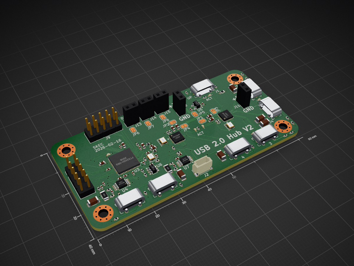
Gridfinity USB hub is an open-source printed circuit board by SK-Electronics-Consulting, from the SK-Electronics-Consulting/electronics-widgets repository on GitHub. It is a 4-layer board of 82 × 40 mm with 124 parts on 152 nets, routed with 1,134 tracks and 180 vias.
It is built around the INA226AIDGSR, CH334F and 93LC56BT-I/OT, with the AP2112K-3.3TRG1, RC0402FR-0710KL and XL-1005UGC among its other parts. Its parts include 38 resistors, 33 capacitors, 15 connectors, 13 diodes and 7 ICs. It belongs with the interfaces and adapters boards of this library.


A 1‑ and 2‑port VNA calibration kit presented at the Murata MM8130‑2600RA2 SWF‑type microwave coaxial switch‑connector interface (DC–6 GHz). Use it to calibrate a cable + Murata probe assembly (or a fixture that uses the SWF/MM8130 probe interface) to the probe tip, so the reference plane lands at the connector's center contact.
Status: V1, 2‑layer, ready for OSH Park. Design‑rule clean (0 DRC, 0 ERC, 0 schematic‑parity).
⚠️ AI‑generated design. This schematic and PCB layout were produced with AI assistance. Review every connection, value, footprint, and dimension against the datasheets before ordering or trusting it. The schematic and the board silkscreen carry the same warning.
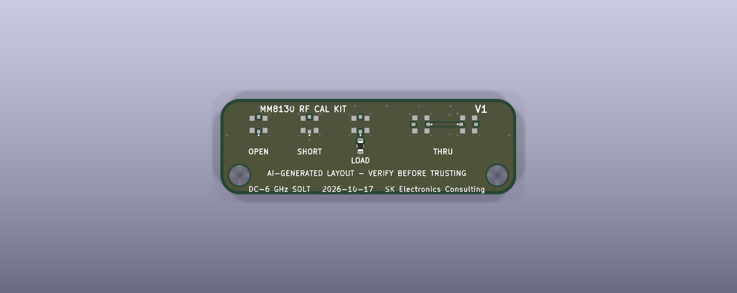
All standards sit on one non‑separable board. Each is an MM8130 receptacle with the standard element placed right at the RF contact. The Murata probe, when inserted, opens the connector's internal switch and contacts pin 1 (IN) — so every standard is defined between IN and GND.
| Ref | Standard | Implementation |
|---|---|---|
| J1 | Open | IN left unterminated (open); defined by the connector's fringing C. |
| J2 | Short | IN tied to the connector's own shell‑ground pads with short, wide copper + a ground via. |
| J3+R1 | Load | 50.0 Ω precision thin‑film RF resistor (Stackpole RNCQ 0603, HF) from IN to GND, placed at the contact. |
| J4↔J5 | Thru | ~50 Ω coplanar‑waveguide line, 5.18 mm IN‑to‑IN, between two MM8130s. |
The switched OUT pin (pin 2) of every connector is intentionally left unconnected — the internal switch isolates it from IN while a probe is inserted, so loading it would only add a stub.
C167503, DigiKey 490‑4981‑1‑ND, Mouser 81‑MM8130‑2600RA2.Custom footprint MM8130:MM8130-2600RA2 (in the project's MM8130.pretty), built from Murata
catalog O30E ("Standard Pattern Dimension") and cross‑checked pad‑for‑pad against the vendor
land pattern (LCSC C167503). Copper lands: two 0.50 × 0.58 mm signal pads (IN/OUT) on the center
axis at ±1.16 mm, and four 0.75 × 0.80 mm ground lands at (±1.025, ±0.95) mm — reproducing the
catalog's 2.80 mm ground span / 1.30 mm signal gap / 2.90 mm signal span.
C167503.| Qty | Value | Footprint | References |
|---|---|---|---|
| 17 | 0.1u | Capacitor_SMD:C_0402_1005Metric | C11, C14, C15, C19, C20, C21, C22, C23, C25, C26, C27, C28, C29, C30, C32, C33 +1 |
| 15 | 10k | Resistor_SMD:R_0402_1005Metric | R6, R7, R8, R9, R10, R11, R12, R13, R20, R22, R23, R32, R33, R34, R35 |
| 13 | Green | LED_SMD:LED_0402_1005Metric | D1, D2, D3, D4, D5, D6, D7, D8, D9, D10, D11, D12, D13 |
| 8 | 10u | Capacitor_SMD:C_0603_1608Metric | C1, C2, C7, C8, C10, C12, C13, C18 |
| 8 | 5.1k | Resistor_SMD:R_0402_1005Metric | R1, R2, R3, R4, R5, R14, R15, R16 |
| 7 | USB_C_Receptacle_USB2.0_16P | Connector_USB:USB_C_Receptacle_G-Switch_GT-USB-7051x | J1, J3, J4, J5, J6, J7, J8 |
| 6 | 47u | Capacitor_SMD:C_1206_3216Metric | C3, C4, C5, C6, C24, C31 |
| 6 | 78.7 | Resistor_SMD:R_0402_1005Metric | R24, R25, R26, R27, R29, R31 |
| 6 | Jumper_2_Small_Bridged | Jumper:SolderJumper-2_P1.3mm_Bridged2Bar_RoundedPad1.0x1.5mm | JP1, JP2, JP5, JP6, JP7, JP8 |
| 5 | Conn_01x02 | Connector_PinSocket_2.54mm:PinSocket_1x02_P2.54mm_Vertical | J11, J12, J13, J14, J15 |
| 4 | 2k | Resistor_SMD:R_0402_1005Metric | R18, R36, R37, R38 |
| 4 | MountingHole_Pad | MountingHole:MountingHole_3.2mm_M3_Pad_Via | H1, H2, H3, H4 |
| 3 | 12MHz | Crystal:Crystal_SMD_2520-4Pin_2.5x2.0mm | Y1, Y2, Y3 |
| 2 | 12k | Resistor_SMD:R_0402_1005Metric | R17, R19 |
| 2 | 12pF | Capacitor_SMD:C_0402_1005Metric | C16, C17 |
| 2 | 5m | Resistor_SMD:R_1206_3216Metric | R28, R30 |
| 2 | CH334F | Package_DFN_QFN:QFN-24-1EP_4x4mm_P0.5mm_EP2.7x2.7mm | U1, U2 |
| 2 | Conn_02x05_Odd_Even | Connector_PinHeader_2.54mm:PinHeader_2x05_P2.54mm_Vertical | J9, J10 |
| 2 | FerriteBead_Small | Inductor_SMD:L_0402_1005Metric | FB1, FB2 |
| 2 | INA226 | Package_SO:TSSOP-10_3x3mm_P0.5mm | U4, U7 |
| 2 | Jumper_2_Small_Open | Jumper:SolderJumper-2_P1.3mm_Open_RoundedPad1.0x1.5mm | JP3, JP4 |
| 1 | 1M | Resistor_SMD:R_0402_1005Metric | R21 |
| 1 | 6V/2A | Resistor_SMD:R_0603_1608Metric | TH1 |
| 1 | 93LC56BxxOT | Package_TO_SOT_SMD:SOT-23-6 | U6 |
| 1 | AP2112K-3.3 | Package_TO_SOT_SMD:SOT-23-5 | U5 |
| 1 | FT2232H-56Q | Package_DFN_QFN:QFN-56-1EP_8x8mm_P0.5mm_EP5.9x5.9mm | U3 |
| 1 | QWIIC | Connector_JST:JST_SH_BM04B-SRSS-TB_1x04-1MP_P1.00mm_Vertical | J2 |
SK-Electronics-Consulting/electronics-widgets
Small, Custom Tools for Electronics

SK-Electronics-Consulting/electronics-widgets
Small, Custom Tools for Electronics

SK-Electronics-Consulting/electronics-widgets
Small, Custom Tools for Electronics

SK-Electronics-Consulting/electronics-widgets
Small, Custom Tools for Electronics

SK-Electronics-Consulting/electronics-widgets
Small, Custom Tools for Electronics

SK-Electronics-Consulting/electronics-widgets
Small, Custom Tools for Electronics

SK-Electronics-Consulting/electronics-widgets
Small, Custom Tools for Electronics

SK-Electronics-Consulting/electronics-widgets
Small, Custom Tools for Electronics

SK-Electronics-Consulting/electronics-widgets
Small, Custom Tools for Electronics

SK-Electronics-Consulting/electronics-widgets
Small, Custom Tools for Electronics

SK-Electronics-Consulting/electronics-widgets
Small, Custom Tools for Electronics

SK-Electronics-Consulting/electronics-widgets
Small, Custom Tools for Electronics


El-Luhb/nvme-Carrier-for-LattePanda-Mu
nvme Carrier PCB for the LattePanda Mu compute module

filliformes/pandore
pandore is an open-source digital audio instrument protyping platform based on the LattePanda Mu.

Tinkerbug-Robotics/TinkerRocket
Model rocket flight computer, ground station, iOS app, and simulation


Haptic-Solutions/MicroPSU
A small but powerful general purpose buck converter.


drandyhaas/KiCadRoutingTools
A set of Python/Rust tools to aid routing in KiCad
It measures 82 × 40 mm and has 4 copper layers, 1.6 mm thick.
124 parts, built around the INA226AIDGSR, CH334F, 93LC56BT-I/OT and AP2112K-3.3TRG1. The full list of its parts is on this page, with links to each part's symbol and footprint where PCBKit's library has them.
From the SK-Electronics-Consulting/electronics-widgets repository on GitHub, at the commit this page was made from: the board is Gridfinity-USB-hub/Gridfinity-USB-hub.kicad_pcb and its schematic Breadboard Power Supply Adapter/Breadboard Power Supply Adapter.kicad_sch. PCBKit opens the board in the browser, with nothing to install.
Its repository states no licence, so its author keeps all rights: ask SK-Electronics-Consulting before reusing the design.