2 layers60 × 30 mm
Controller
google/mozc-devices
Circuit diagrams and firmware source code for Gboard DIY keyboards
11 parts3kApache-2.0
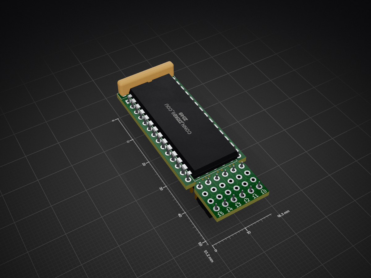
 RetroStack/MCM776x_CharGen_Adapter10
Hardware adapter to replace a MCM776x character generator with a ROM (e.g. MCM7760, MMC7764 used in TRS-80 Model 1)
MCM776x Character Generator Adapter is an open-source printed circuit board by RetroStack, from the RetroStack/MCM776x_CharGen_Adapter repository on GitHub, published under the MIT licence. It is a 2-layer board of 18.3 × 51.2 mm with 11 parts on 27 nets, routed with 312 tracks and 11 vias.
Its parts include 2 ICs and 2 connectors. It belongs with the interfaces and adapters boards of this library.
This repository provides an adapter for the Motorola MCM6670 and related (MCM667x series) character generators for vintage computers. ROMs with various character sets are provided in a separate repository. The entire project is available under the MIT license.
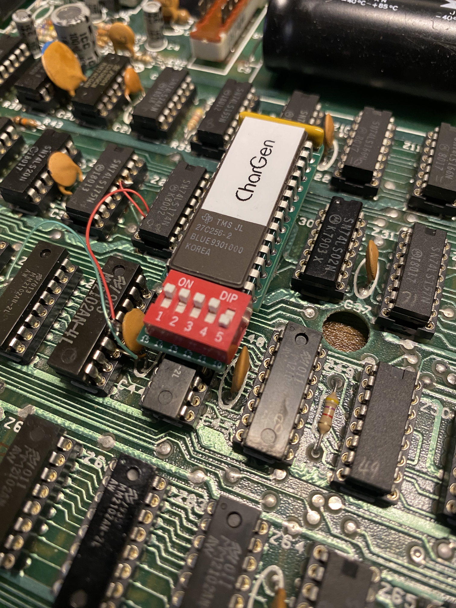
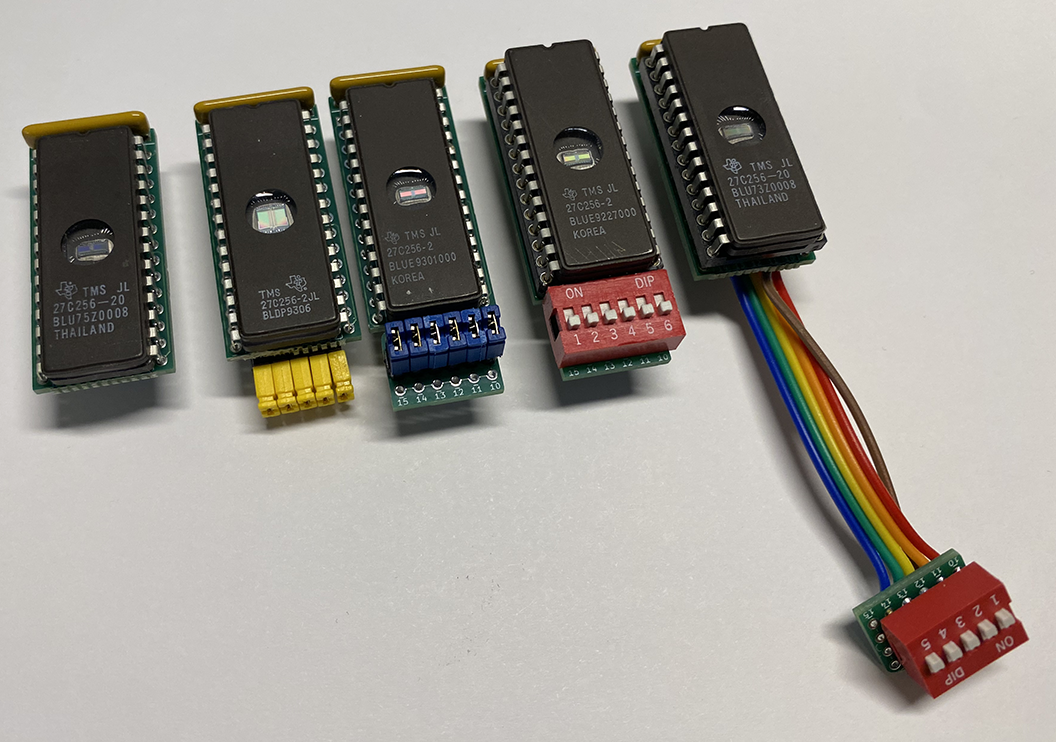
In the "Latest" folder, you'll find the most up-to-date design files, including:
The adapter has been implemented using KiCAD 7. The KiCAD project files are included in this repository.
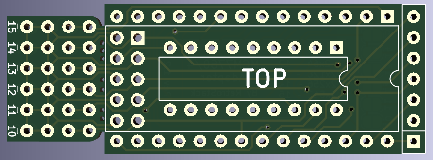
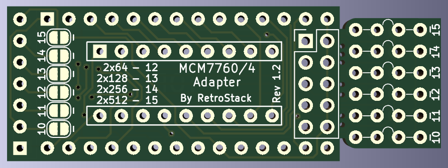
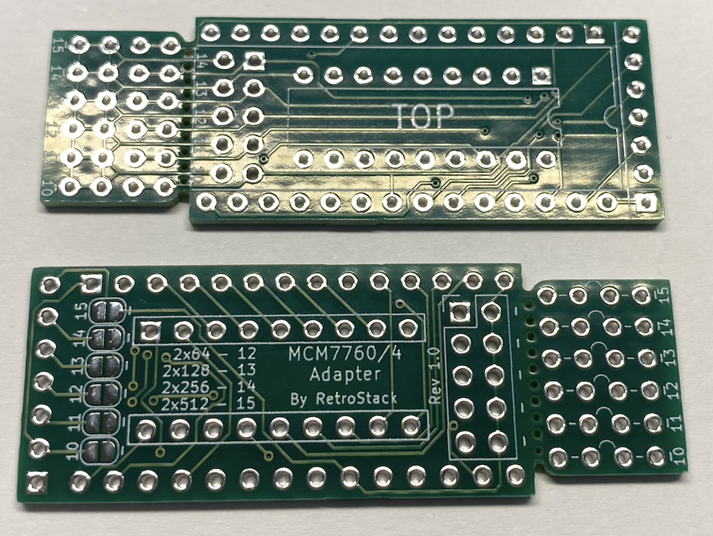
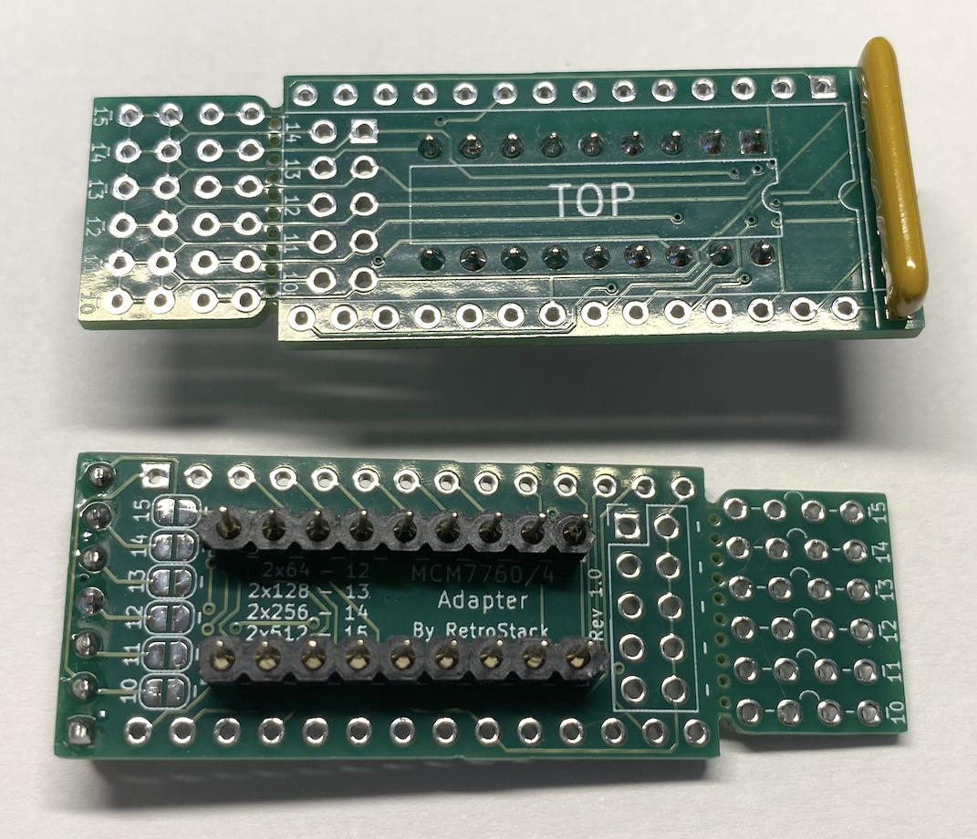
The adapter provides various configurations. Depending on your ROM used, only some PINs can be configured. See the description on the board for more details. For example, a 27256 ROM only uses 14 pins and therefore only 5 pins can be configured. The 6th will not have an affect.
NOTE: Keep in mind that the bits are active-low. That means if you want to put set a 1 on a specific address, you leave it unbridged. If you want a 0, then bridge it. This can be fixed by using a reversed/inverted ROM. See below for more details why that is.
NOTE: The board exposes the bits from right to left. If you prefer left to right (e.g. for DIP switches to match labels), then flip the address bits in the ROM or use the provided "f" versions of these.
Here are some examples:
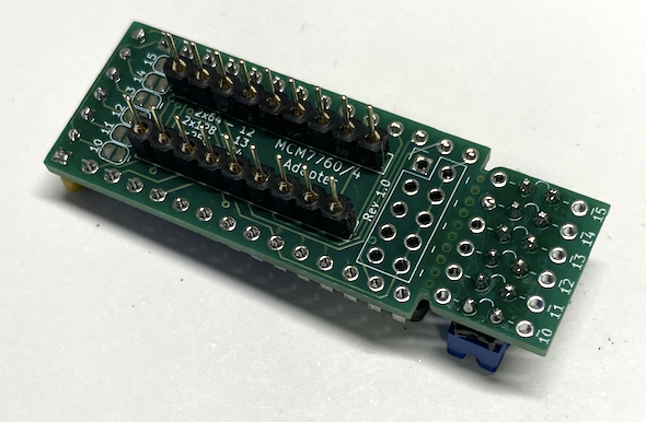
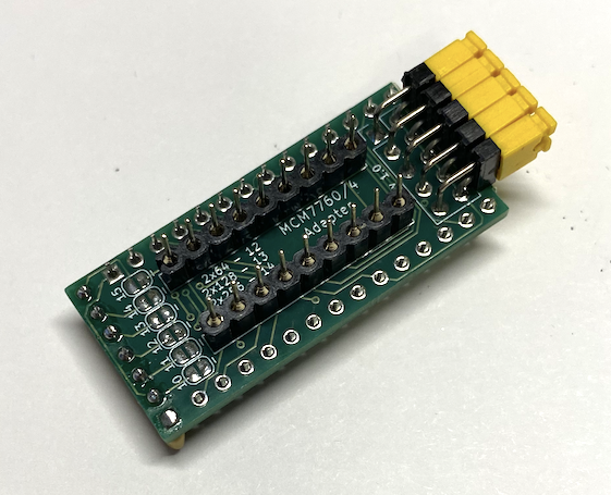
NOTE: Due to space constraints, only 5 jumpers can be used. 7) Clip off extension board on perforated line. 8) Add a 2 row pin right-angle header (2.54mm pitch) to the bottom of the PCB, extending one end out over the board where the extension was. 8) Add jumpers.
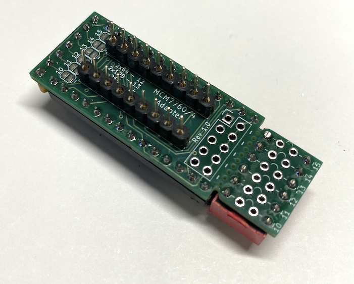
NOTE: For TRS-80 Model 1: Use low-profile dip switches to make sure the adapter fits in the case. 7) Add a DIP switch on the extension board. The DIP switch should cover all holes from front to back.
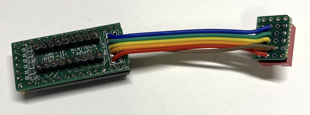
NOTE: Due to space constraints, only 5 DIP switches can be used. 7) Clip off extension board on perforated line. 8) Solder up to 6 wires (e.g. ribbon cable) to the bottom of the PCB. Use up to 5 wires for each address line, which is the row close to the center of the board (next to the revision number). To identify which address line is which, see the label just below the ROM on the top of the adapter PCB. Solder at least one wire to any of the holes closer to the edge of the board. These are ground pins and therefore any could be used. 9) Solder all wires to the extension board. Use the central two rows of holes. Solder it on from the bottom as DIP switches will be added to the top. Solder the address lines closest to the perforated line where the extension board was attached to the adapter PCB. Solder the single ground wire to and other hole of the second row of holes further away from the perforated edge. 10) Add a DIP switch on the extension board. The DIP switch should cover all holes from front to back. You may need to trim the soldered pins of the cable to solder the DIP switches as close to flush as possible.
NOTE: Due to space constraints, only 5 jumpers can be used. 7) Clip off extension board on perforated line. 8) Solder up to 6 wires (e.g. ribbon cable) to the bottom of the PCB. Use up to 5 wires for each address line, which is the row close to the center of the board (next to the revision number). To identify which address line is which, see the label just below the ROM on the top of the adapter PCB. Solder at least one wire to any of the holes closer to the edge of the board. These are ground pins and therefore any could be used. 9) Add a 2 row pin straight header (2.54mm pitch) to the center two pins of the extension board. You need to leave one row on each side (on edge and on the side next to the ROM). 10) Solder all wires to the extension board. Use the row closer to the perforated edge to solder the address lines. Solder the single ground wire to and other hole at the bottom edge furthest away from the perforated edge. You can solder it from the top or bottom. 11) Add jumpers.
Some ROMs, especially the EEPROMs have an active-low WRITE pin that needs to be HIGH (or 1) in normal (read) use. To avoid putting ROMs in an incorrect mode (write mode instead of read mode), all additional pins are pulled high by default through pull-up resistors.
Having them in this orientation was the simplest without adding complexity to the design. Additionally, the addressing depends on what type of configuration you use. Binary numbers are usually written from right to left (as implemented) and this works best for jumpers, for example. However, DIP switches uses labels from left to right. Overall, one direction had to be chosen, and I went with the simplest. This can be fixed by flipping the address bits. ROMs having this fix already marked with an "f".
Below is a list of materials needed to assemble a complete system. Please note that the links and prices (scroll to the right to see them; as of March 3rd, 2024) will not be updated in the future and should only be used as a reference for locating the correct items.
NOTE: Links and alternatives are provided to assist you in finding the necessary components. I cannot guarantee the complete accuracy or reliability of all these links and alternatives. Please check it for yourself!
| PCB REFERENCE | QTY | VALUE | COMMENT | EACH | TOTAL | SOURCE LINK |
|---|---|---|---|---|---|---|
| RN1 | 1 | 4.7k Ohm | 6 resistor network with 7-pins, bussed resistors | 0.5 | 0.5 | Mouser |
| U1 | 2 | Source Link is for a rather expensive version of a machined straight male pin header with 40-pins which can be broken into smaller pieces to server for both. There are cheaper ones, but the link is used for future reference. | 1.0 | 1.0 | Mouser | |
| U2 | 1 | 2x64-2x512 | Examples are 23128, 23256, 2764, 27128, 27256, 27512, 2864, 28256 and all other variations such as 27C256 or AT28C64B | 5.5 | 5.5 | Mouser |
| J1 | 1 | - | Optional. Could be used for right-angle jumpers or attaching ribbon cable to move switch towards more accessible place. | 1.02 | 1.02 | Mouser |
| J2 | 1 | - | Optional. Adding the ability to switch character sets. | 0.27 | 0.27 | Mouser |
| 1 | Low-profile | Optional. Adding the ability to switch character sets. | 0.67 | 0.67 | Mouser |
To work with this KiCAD project, you'll need the RetroStack libraries for KiCAD. Please follow this link to access and install these libraries.
RetroStack is passionate about exploring and preserving the legacy of older computer systems. My work involves creating detailed documentation and videos to share the knowledge. I am also dedicated to reviving these classic systems by reimplementing them and offering replacement parts at no cost. If you're keen on supporting this unique project, I invite you to visit my Patreon page. Your support would be immensely valuable and greatly appreciated!
This project is licensed under the MIT License - see the LICENSE file for details.
| Qty | Value | Footprint | References |
|---|---|---|---|
| 6 | SolderJumper_2_Open | RetroStackLibrary:SolderJumper_2_Open_RoundedPad | JP1, JP2, JP3, JP4, JP5, JP6 |
| 1 | 27512 | Package_DIP:DIP-28_W15.24mm | U2 |
| 1 | Conn_02x05_Odd_Even | Connector_PinHeader_2.54mm:PinHeader_2x05_P2.54mm_Vertical | J1 |
| 1 | Conn_02x06_Odd_Even | RetroStackLibrary:DIPJumper_6 | J2 |
| 1 | Conn_02x09_Counter_Clockwise | Package_DIP:DIP-18_W7.62mm | U1 |
| 1 | R_Network06 | Resistor_THT:R_Array_SIP7 | RN1 |
google/mozc-devices
Circuit diagrams and firmware source code for Gboard DIY keyboards


FrameworkComputer/ExpansionCards
Reference designs and documentation to create Expansion Cards for the Framework Laptop

hoglet67/RGBtoHDMI
Bare-metal Raspberry Pi project that provides pixel-perfect sampling of Retro Computer RGB/YUV video and conversion to HDMI

hackclub/OnBoard
💡 Join 1,000 teenagers and make your first PCB with a $100 grant!


tardate/LittleArduinoProjects
a collection of "Little Electronic & Arduino Projects", most involving electronics or an Arduino in one way or another!

basilfx/TRADFRI-Hacking
Hacking IKEA TRÅDFRI products, such as light bulbs, window blinds and other accessories.
It measures 18.3 × 51.2 mm and has 2 copper layers, 1.6 mm thick.
11 parts. The full list of its parts is on this page, with links to each part's symbol and footprint where PCBKit's library has them.
From the RetroStack/MCM776x_CharGen_Adapter repository on GitHub, at the commit this page was made from: the board is KiCAD/MCM776x_Character_Generator_Adapter.kicad_pcb and its schematic KiCAD/MCM776x_Character_Generator_Adapter.kicad_sch. PCBKit opens the board in the browser, with nothing to install.
Its repository publishes it under the MIT licence: you may reuse it on that licence's terms (keep the author's notice, and for a copyleft licence share your changes alike).