
2 layers171.2 × 72.9 mm
Amiga gfxcard old
mntmn/amiga2000-gfxcard
MNT VA2000, an Open Source Amiga 2/3/4000 Graphics Card (Zorro II/III), written in Verilog
34 parts1k
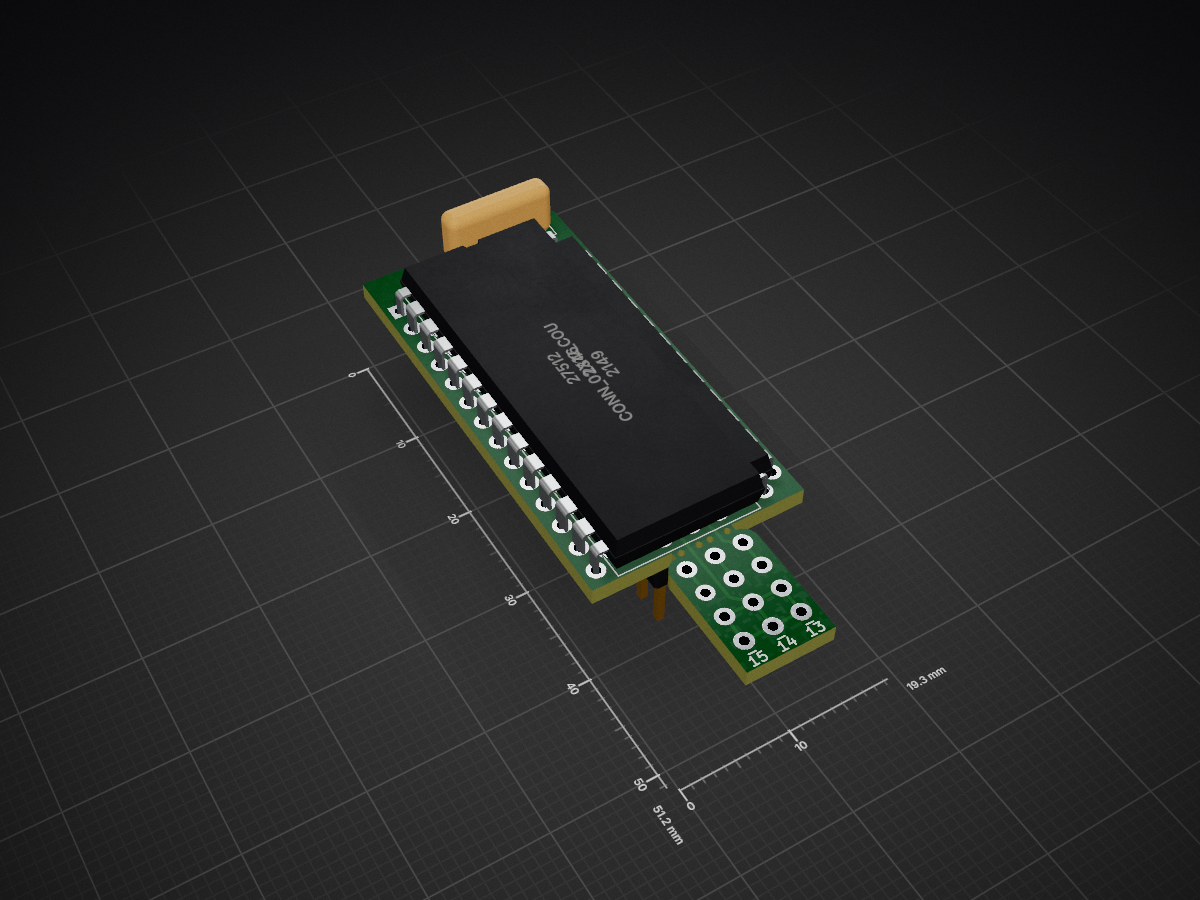
 RetroStack/2332_2364-ROM_Adapter7
Compact and universal 2332 and 2364 ROM adapter
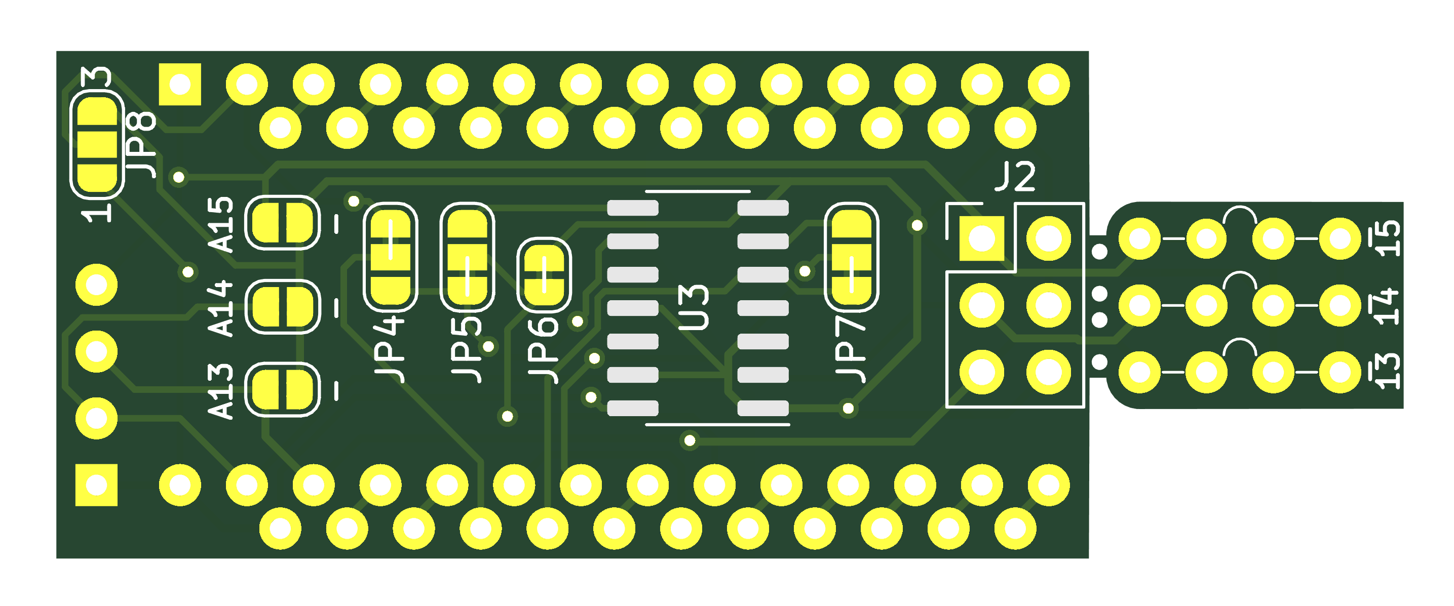
2332 2364-ROM Adapter is an open-source printed circuit board by RetroStack, from the RetroStack/2332_2364-ROM_Adapter repository on GitHub, published under the MIT licence. It is a 2-layer board of 19.3 × 51.2 mm with 14 parts on 37 nets, routed with 227 tracks and 12 vias.
It is built around the 74LS04PC. Its parts include 3 ICs and 2 connectors. It belongs with the interfaces and adapters boards of this library.
This repository provides an adapter for 2332 and 2364 ROMs for vintage computers. With an optional hidden inverter chip on the bottom, all versions of these boards can be emulated. The adapter was designed to have the smallest possible footprint while still using through-hole components for a vintage look. It includes an optional detachable selector board for DIP switches or jumpers. Without the detachable selector board, solder jumpers can be used instead. The provided pads on the bottom allow for synchronized address selection across multiple adapters. The entire project is available under the MIT license.
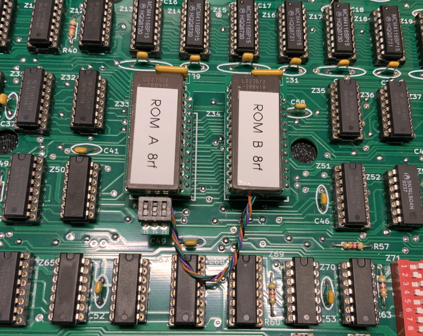
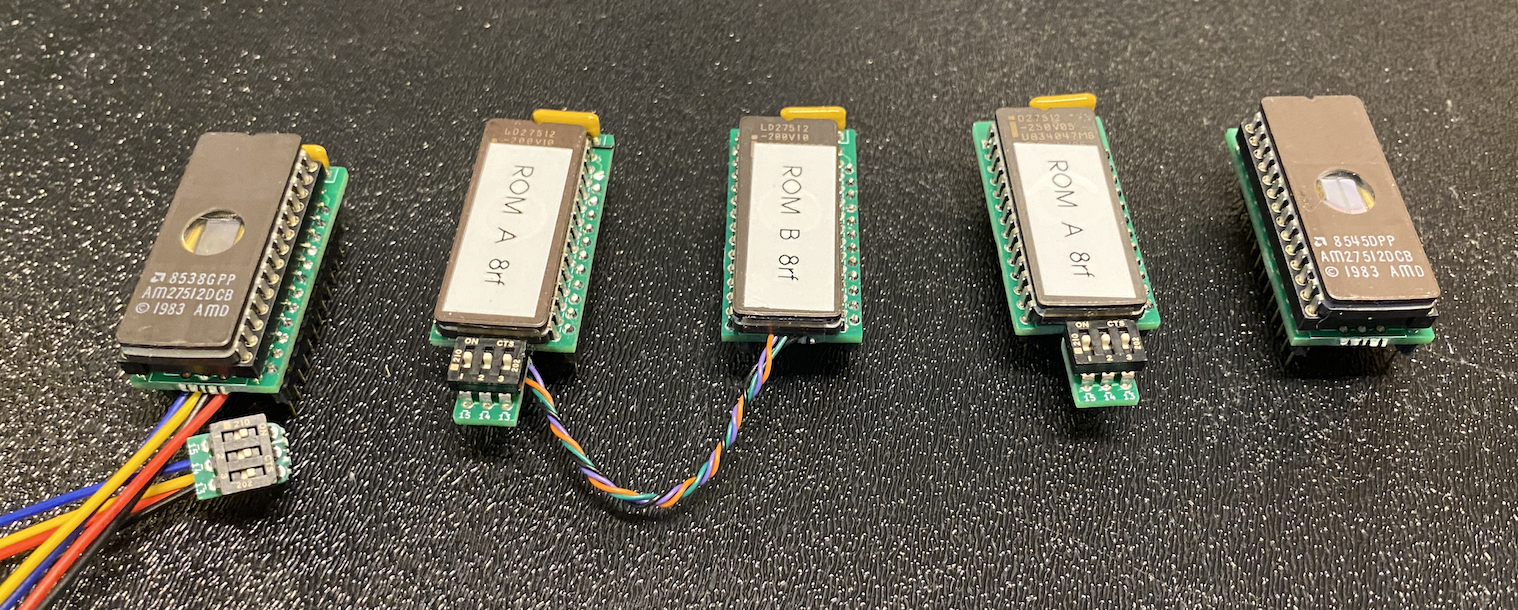
In the "Latest" folder, you'll find the most up-to-date design files, including:
The adapter has been implemented using KiCAD 7. The KiCAD project files are included in this repository.
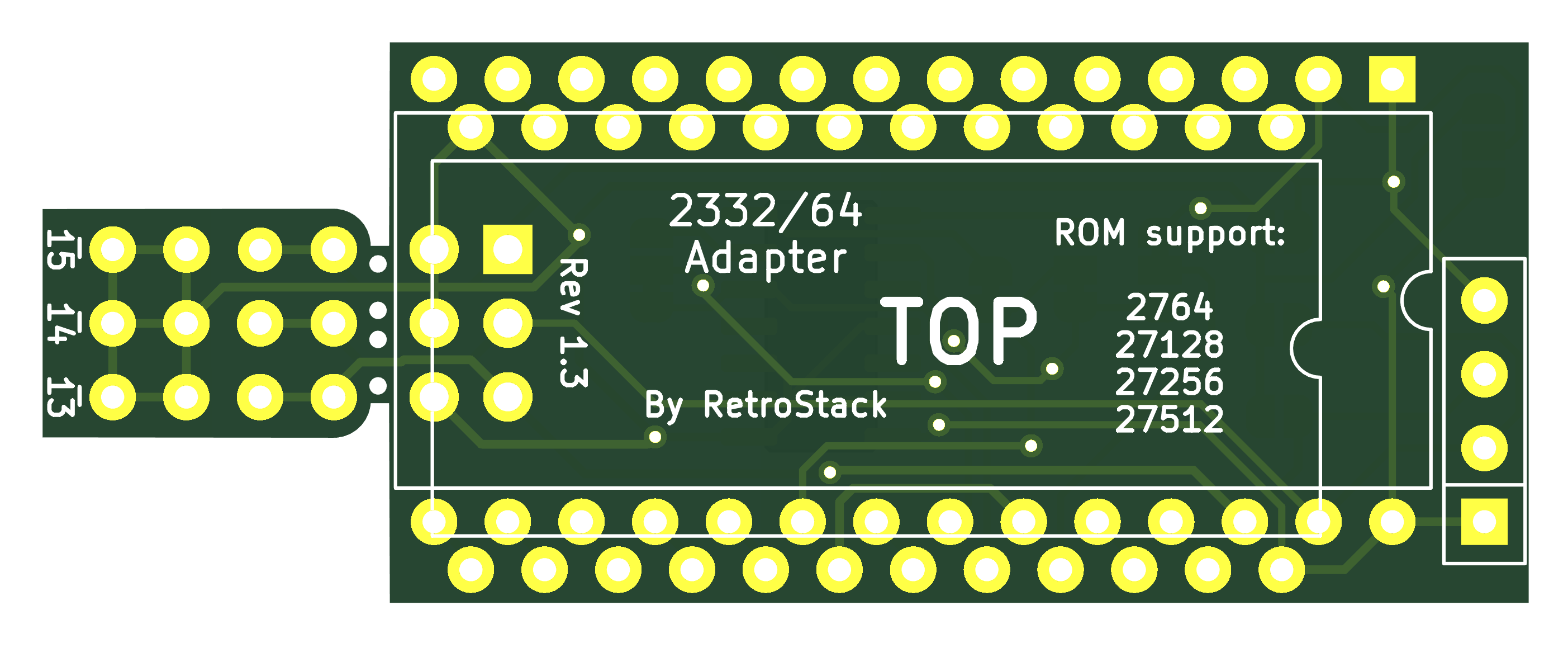
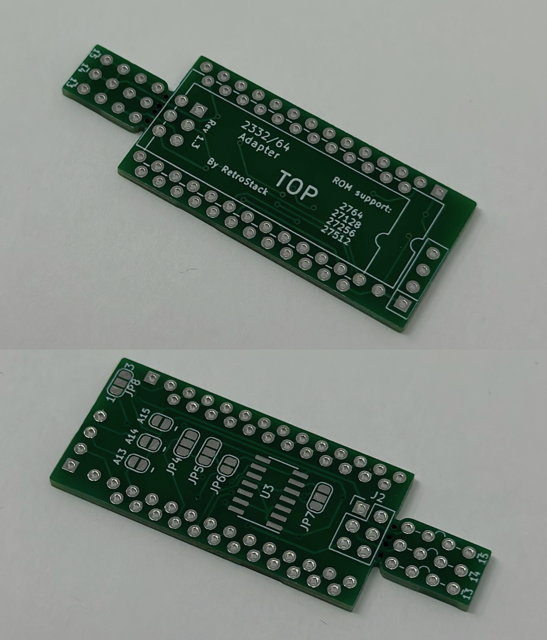
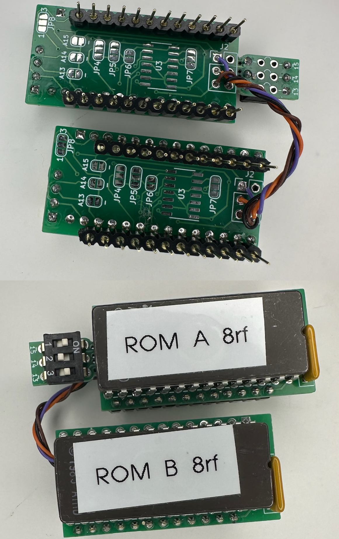
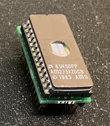
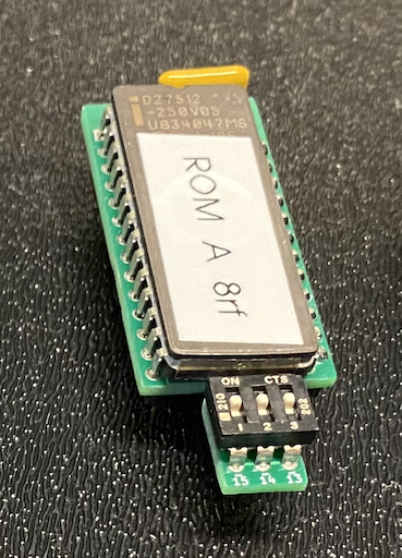
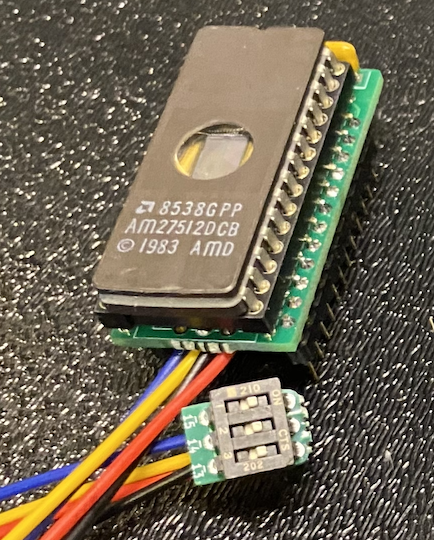
The adapter allows for bank-switching of various ROMs. Depending on the size of the ROM used, only certain pins may be configurable. For example, a 27256 ROM has 15 address pins. The adapter exposes 13 of these pins to the bottom pins, leaving 2 additional address lines available for bank-switching. A 27512 would then have 3 additional address lines.
NOTE: Keep in mind that the bits are active-low. This means that if you want to set a 1 on a specific address, you leave it unbridged. If you want a 0, you should bridge it. See below for more details on why it was designed this way.
NOTE: The board exposes the bits from right to left. If you prefer left to right (e.g., for DIP switches to match labels), you can flip the address bits in the ROM or use the provided "f" versions in the systems ROM repository.
Here are some examples of available bank-switching configurations:
NOTE: For the TRS-80 Model 1, use low-profile DIP switches to ensure the adapter fits inside the case. 7) Add a DIP switch to the extension board. The DIP switch should cover all holes from front to back.
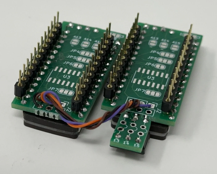
Sometimes it is useful to be able to bank-switch multiple ROMs simultaneously.
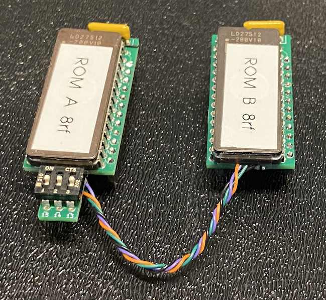
Depending on which ROM and even the specific version you want to emulate, you will need to configure the adapter accordingly. Below is a list of configurations:
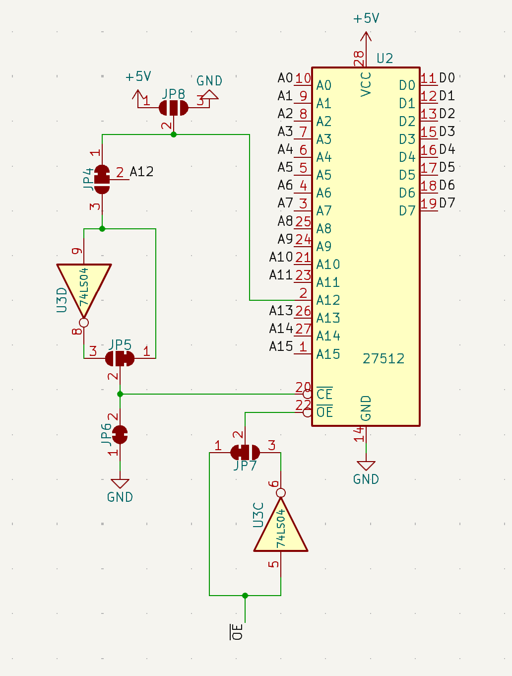
This is the default configuration. No additional steps are required.
Some ROMs, especially EEPROMs, have an active-low WRITE pin that needs to be HIGH (or 1) during normal (read) use. To prevent accidentally putting ROMs into the incorrect mode (write mode instead of read mode), all additional pins are pulled high by default through pull-up resistors.
Having them in this orientation was the simplest solution without adding complexity to the design. Additionally, the addressing depends on the type of configuration you use. Binary numbers are typically written from right to left (as implemented), which works best for jumpers, for example. However, DIP switches use labels from left to right.
Overall, one direction had to be chosen, and I opted for the simplest. This can be adjusted by flipping the address bits. ROMs with this fix are already marked with an "f".
Below is a list of materials needed to assemble a complete system. Please note that the links and prices (scroll to the right to see them; as of August 22nd, 2024) will not be updated in the future and should only be used as a reference for locating the correct items.
NOTE: Links and alternatives are provided to assist you in finding the necessary components. I cannot guarantee the complete accuracy or reliability of all these links and alternatives. Please verify the information for yourself.
| PCB REFERENCE | QTY | VALUE | COMMENT | EACH | TOTAL | SOURCE LINK |
|---|---|---|---|---|---|---|
| RN1 | 1 | 4.7k Ohm | 3 resistor network with 4-pins, bussed resistors | 0.35 | 0.35 | Mouser |
| U1 | 2 | Source Link is for a rather expensive version of a machined straight male pin header with 40-pins which can be broken into smaller pieces to server for both. There are cheaper ones, but the link is used for future reference. | 1.0 | 1.0 | Mouser | |
| U2 | 1 | 2x64-2x512 | Examples are 23128, 23256, 2764, 27128, 27256, 27512, 2864, 28256 and all other variations such as 27C256 or AT28C64B | 5.5 | 5.5 | Mouser |
| U3 | 1 | 74LS04 | Optional. Needed for inverting chip select pins. | 0.68 | 0.68 | Mouser |
| J1 | 1 | - | Optional. Could be used for right-angle jumpers or attaching ribbon cable to move switch towards more accessible place. | 1.02 | 1.02 | Mouser |
| J2 | 1 | - | Optional. Adding the ability to switch character sets. | 0.27 | 0.27 | Mouser |
| 1 | Low-profile | Optional. Adding the ability to switch character sets. | 0.67 | 0.67 | Mouser |
This repository contains only the adapter boards. The ROM binaries themselves can be found in other repositories and sources. Below is a list of known binary sources:
More sources will be added over time. Let me know if you are aware of good sources.
To work with this KiCAD project, you'll need the RetroStack libraries for KiCAD. Please follow this link to access and install these libraries.
RetroStack is passionate about exploring and preserving the legacy of older computer systems. My work involves creating detailed documentation and videos to share the knowledge. I am also dedicated to reviving these classic systems by reimplementing them and offering replacement parts at no cost. If you're keen on supporting this unique project, I invite you to visit my Patreon page. Your support would be immensely valuable and greatly appreciated!
This project is licensed under the MIT License - see the LICENSE file for details.
| Qty | Value | Footprint | References |
|---|---|---|---|
| 3 | SolderJumper_2_Open | RetroStackLibrary:SolderJumper_2_Open_RoundedPad | JP1, JP2, JP3 |
| 3 | Switch for 2332! | Jumper:SolderJumper-3_P1.3mm_Bridged12_RoundedPad1.0x1.5mm_NumberLabels | JP4, JP5, JP7 |
| 1 | 27512 | Package_DIP:DIP-28_W15.24mm | U2 |
| 1 | 74LS04 | Package_SO:SOIC-14_3.9x8.7mm_P1.27mm | U3 |
| 1 | Conn_02x03_Odd_Even | Connector_PinHeader_2.54mm:PinHeader_2x03_P2.54mm_Vertical | J2 |
| 1 | Conn_02x03_Odd_Even | RetroStackLibrary:DIPJumper_3 | J1 |
| 1 | Conn_02x12_Counter_Clockwise | Package_DIP:DIP-24_W15.24mm | U1 |
| 1 | R_Network03 | Resistor_THT:R_Array_SIP4 | RN1 |
| 1 | SolderJumper_2_Bridged | Jumper:SolderJumper-2_P1.3mm_Bridged_RoundedPad1.0x1.5mm | JP6 |
| 1 | SolderJumper_3_Open | Jumper:SolderJumper-3_P1.3mm_Open_RoundedPad1.0x1.5mm_NumberLabels | JP8 |
mntmn/amiga2000-gfxcard
MNT VA2000, an Open Source Amiga 2/3/4000 Graphics Card (Zorro II/III), written in Verilog

Redherring32/OpenTendo
An Open-Source HardWare (OSHW) recreation of the original 1985 front-loading NES Motherboard

jotego/jtcores
FPGA cores compatible with multiple arcade game machines and KiCAD schematics of arcade games. Working on MiSTer FPGA/Analogue Pocket

jes/scamp-cpu
A homebrew 16-bit CPU with a homebrew Unix-like-ish operating system.


Nakazoto/CenturionComputer
This is just a simple backup of all the files related to the Centurion that I have stored on my HD. The Wiki itself has far more in-depth information about the Centurion and it's individual cards.


The-Invent0r/8-bit-Computer-PCB
These are the KiCAD files for my 8-Bit Computer.
It measures 19.3 × 51.2 mm and has 2 copper layers, 1.6 mm thick.
14 parts, built around the 74LS04PC. The full list of its parts is on this page, with links to each part's symbol and footprint where PCBKit's library has them.
From the RetroStack/2332_2364-ROM_Adapter repository on GitHub, at the commit this page was made from: the board is KiCAD/2332_2364_ROM_Adapter.kicad_pcb and its schematic KiCAD/2332_2364_ROM_Adapter.kicad_sch. PCBKit opens the board in the browser, with nothing to install.
Its repository publishes it under the MIT licence: you may reuse it on that licence's terms (keep the author's notice, and for a copyleft licence share your changes alike).