2 layers27 × 20 mm
Ionto Current Source Core With Pour
Pluze/pcb
Reference and experimental KiCad PCB designs with reusable agent workflows
8 partsMIT
 Pluze/pcb
Reference and experimental KiCad PCB designs with reusable agent workflows
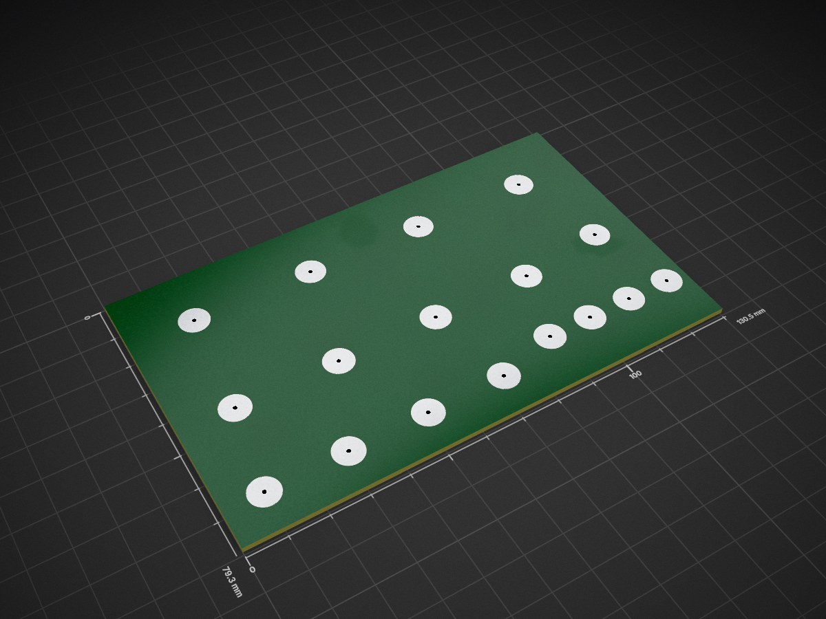
Snap Adapter 17up 150x100 is an open-source printed circuit board by Pluze, from the Pluze/pcb repository on GitHub, published under the MIT licence. It is a 2-layer board of 130.5 × 79.3 mm with 17 parts on 17 nets.
It belongs with the interfaces and adapters boards of this library.
This design family adapts circular thin-film electrodes to an exposed front copper pad intended for soldering a snap connector. Each board has one centered contact on each side and one centered drilled hole. The front contact is fixed at 8 mm; the back contact follows the thin-film electrode diameter.
The boards are intended for in-house fabrication on an LPKF U4. The machine does not create a plated barrel in this workflow, so the center hole is a manual interconnect: wick solder through the 1.0 mm drill to join the front and back copper, then verify continuity before attaching the film electrode.
| Variant file | Front snap pad | Back film-electrode pad | Square board | Limiting copper-to-edge margin |
|---|---|---|---|---|
Circular_Contact_F8_B5_S10.kicad_pcb | 8 mm | 5 mm | 10 mm | 1 mm |
Circular_Contact_F8_B10_S18p75.kicad_pcb | 8 mm | 10 mm | 18.75 mm | 4.375 mm |
Circular_Contact_F8_B15_S25.kicad_pcb | 8 mm | 15 mm | 25 mm | 5 mm |
Circular_Contact_F8_B20_S30.kicad_pcb | 8 mm | 20 mm | 30 mm | 5 mm |
| Variant | Front | Back |
|---|---|---|
| 8/5/10 |  |  |
| 8/10/18.75 |  |  |
| 8/15/25 |  |  |
| 8/20/30 |  |  |
The 20/30 mm, 15/25 mm, and 10/18.75 mm pairs are taken from the centered circle/square geometry in electrode-size-test.dxf. The source also explicitly labels a 5 mm electrode but does not contain a completed centered square for it; the 10 mm minimum board requested for this project is therefore used for the 5 mm variant.
F.Cu/F.Mask, with no paste aperture.B.Cu/B.Mask, with no paste aperture.CONTACT via in KiCad.The base project PCB is the largest 8/20/30 mm member. The four independently manufacturable family members are under variants/. The schematic is intentionally empty because this is a geometry-defined, single-net passive adapter.
panels/Snap_Adapter_17up_150x100.kicad_pcb places 17 adapters on one 150 x 100 mm raw FR4 sheet while retaining at least three copies of every family member. Finished outlines are separated by 2 mm:
This yields four 30 mm, four 25 mm, five 18.75 mm, and four 10 mm boards. The finished-board area is 8,257.8125 mm², or 55.05% of the raw material area, compared with 39.53% for exactly three of each. The 17 coupon-cut contours occupy a 129 x 77.75 mm bounding box. A single 130.5 x 79.25 mm processing boundary surrounds them with a 0.75 mm rail and is the only geometry on Edge.Cuts. CircuitPro's documented automatic-fiducial example uses 1.5 mm fiducials whose centers are 4 mm outside BoardOutline, so the corresponding outside envelope is 140 x 88.75 mm. Centering leaves 5 mm horizontally and 5.625 mm vertically from the fiducial outer edges to the material edges.
The dashed 150 x 100 mm stock outline and four expected fiducial circles in the KiCad panel are on Dwgs.User; they are visual planning aids only. The seventeen finished coupon contours are on User.1 (Coupon.Cuts) so they can be imported separately from the continuous BoardOutline. Import the five panel machine files, then let CircuitPro create the actual fiducials from BoardOutline at 4 mm distance. Do not assign Dwgs.User as a manufacturing layer.
| Front | Back |
|---|---|
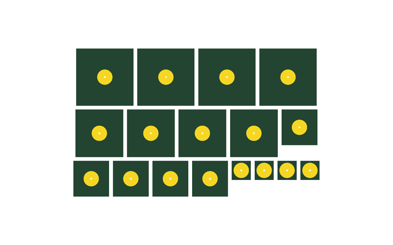 | 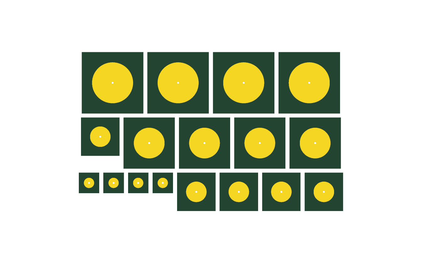 |
These reader-facing previews show the seventeen finished coupons after separation. They are rendered from a temporary view-only copy that maps Coupon.Cuts to board outlines and omits the continuous processing rail; the manufacturing PCB and exported layer mapping remain unchanged.
The active build target is the 17-coupon panel under
fabrication/u4/Snap_Adapter_17up_150x100/.
Import its five machine files together: TopLayer.gtl → TopLayer,
BottomLayer.gbl → BottomLayer, BoardOutline.gm1 → BoardOutline,
CutInside.gm2 → CutInside, and DrillPlated.drl → DrillPlated. Keep the continuous
processing outline separate from the 17 coupon contours. Use the qualified U4
recipe for complete copper removal and double-sided registration, then perform
the non-plated center-hole solder operation described above. Standalone coupon
sources are under variants/; the build publishes the panel as the active target.
fabrication/lightburn/ contains millimetre DXF files generated from F.Mask or B.Mask together with Edge.Cuts. Import the DXF for the required side into LightBurn. Front files are top-view geometry; back files remain in KiCad board coordinates, so apply LightBurn's horizontal flip only when the chosen tape-transfer orientation requires it. Laser settings are intentionally not stored in these geometry files.
From the repository root:
python3 tools/pcbflow/routing/scripts/generate_circular_contact_board.py \
  --csv Designs/Electrode_Snap_Adapter_Series/series.csv \
  --output-dir Designs/Electrode_Snap_Adapter_Series/variants \
  --via-diameter 2 \
  --via-drill 1 \
  --force
Regenerate the base project board:
python3 tools/pcbflow/routing/scripts/generate_circular_contact_board.py \
  8 20 30 \
  --output-dir Designs/Electrode_Snap_Adapter_Series \
  --name Electrode_Snap_Adapter_Series \
  --via-diameter 2 \
  --via-drill 1 \
  --force
Regenerate the 17-adapter panel:
python3 tools/pcbflow/routing/scripts/generate_circular_contact_panel.py \
  --csv Designs/Electrode_Snap_Adapter_Series/series.csv \
  --output Designs/Electrode_Snap_Adapter_Series/panels/Snap_Adapter_17up_150x100.kicad_pcb \
  --count-each 3 --gap 2 \
  --stock-width 150 --stock-height 100 \
  --fiducial-distance 4 --fiducial-diameter 1.5 --stock-edge-margin 5 \
  --processing-rail 0.75 \
  --row 30:4 \
  --row 25:4,18.75:1 \
  --row 18.75:4,10:4 \
  --via-diameter 2 --via-drill 1 \
  --force
Regenerate or audit the U4 and LightBurn manufacturing outputs directly from the KiCad PCB files:
python3 tools/pcbflow/kicad/scripts/export_circuitpro_u4_packages.py \
  export Designs/Electrode_Snap_Adapter_Series --force
python3 tools/pcbflow/kicad/scripts/export_kapton_lightburn_templates.py \
  export Designs/Electrode_Snap_Adapter_Series --force
For another size, the only required geometry inputs remain FRONT_DIAMETER BACK_DIAMETER BOARD_SIDE. Keep the front value at 8 mm for this snap-connector family unless the connector changes.
The 10 mm board has only 1 mm copper-to-edge margin around the 8 mm front pad. It meets the stated minimum size but is the least tolerant of cutter runout, registration error, and edge damage.
./pcb build --design Electrode_Snap_Adapter_Series refreshes U4, LightBurn DXF and
fabrication/gerber/ together. Each supplier package includes
all declared layers, the native Gerber job, PTH/NPTH drill files and PACKAGE.md
with layer mapping and order parameters to confirm. For the complete saved-design
routing workflow, use the repository tool guide.
| Qty | Value | Footprint | References |
|---|---|---|---|
| 5 | FRONT_8mm_BACK_10mm | Circular_Contact_Asymmetric | J9, J10, J11, J12, J13 |
| 4 | FRONT_8mm_BACK_15mm | Circular_Contact_Asymmetric | J5, J6, J7, J8 |
| 4 | FRONT_8mm_BACK_20mm | Circular_Contact_Asymmetric | J1, J2, J3, J4 |
| 4 | FRONT_8mm_BACK_5mm | Circular_Contact_Asymmetric | J14, J15, J16, J17 |
Pluze/pcb
Reference and experimental KiCad PCB designs with reusable agent workflows

Pluze/pcb
Reference and experimental KiCad PCB designs with reusable agent workflows


hoglet67/RGBtoHDMI
Bare-metal Raspberry Pi project that provides pixel-perfect sampling of Retro Computer RGB/YUV video and conversion to HDMI


hackclub/OnBoard
💡 Join 1,000 teenagers and make your first PCB with a $100 grant!

DDeGonge/OS-ARM
This arm is not industrial and it will not be fast, but that is not my goal. But it will hopefully be a very nice looking arm fully capable of 6dof motion, cheap enough to keep it accessable but capable enough to…


It measures 130.5 × 79.3 mm and has 2 copper layers, 1.6 mm thick.
17 parts. The full list of its parts is on this page, with links to each part's symbol and footprint where PCBKit's library has them.
From the Pluze/pcb repository on GitHub, at the commit this page was made from: the board is Designs/Electrode_Snap_Adapter_Series/panels/Snap_Adapter_17up_150x100.kicad_pcb and its schematic Designs/Electrode_Snap_Adapter_Series/Electrode_Snap_Adapter_Series.kicad_sch. PCBKit opens the board in the browser, with nothing to install.
Its repository publishes it under the MIT licence: you may reuse it on that licence's terms (keep the author's notice, and for a copyleft licence share your changes alike).