


4 layers75 × 55 mm
Eos epu up5k
embeddedos-org/eCAD-Hardware-Products
Hardware designs + EE docs + Board datasheets of Multiple products
145 parts8MIT

 PaulBichl/VibePCB-LA
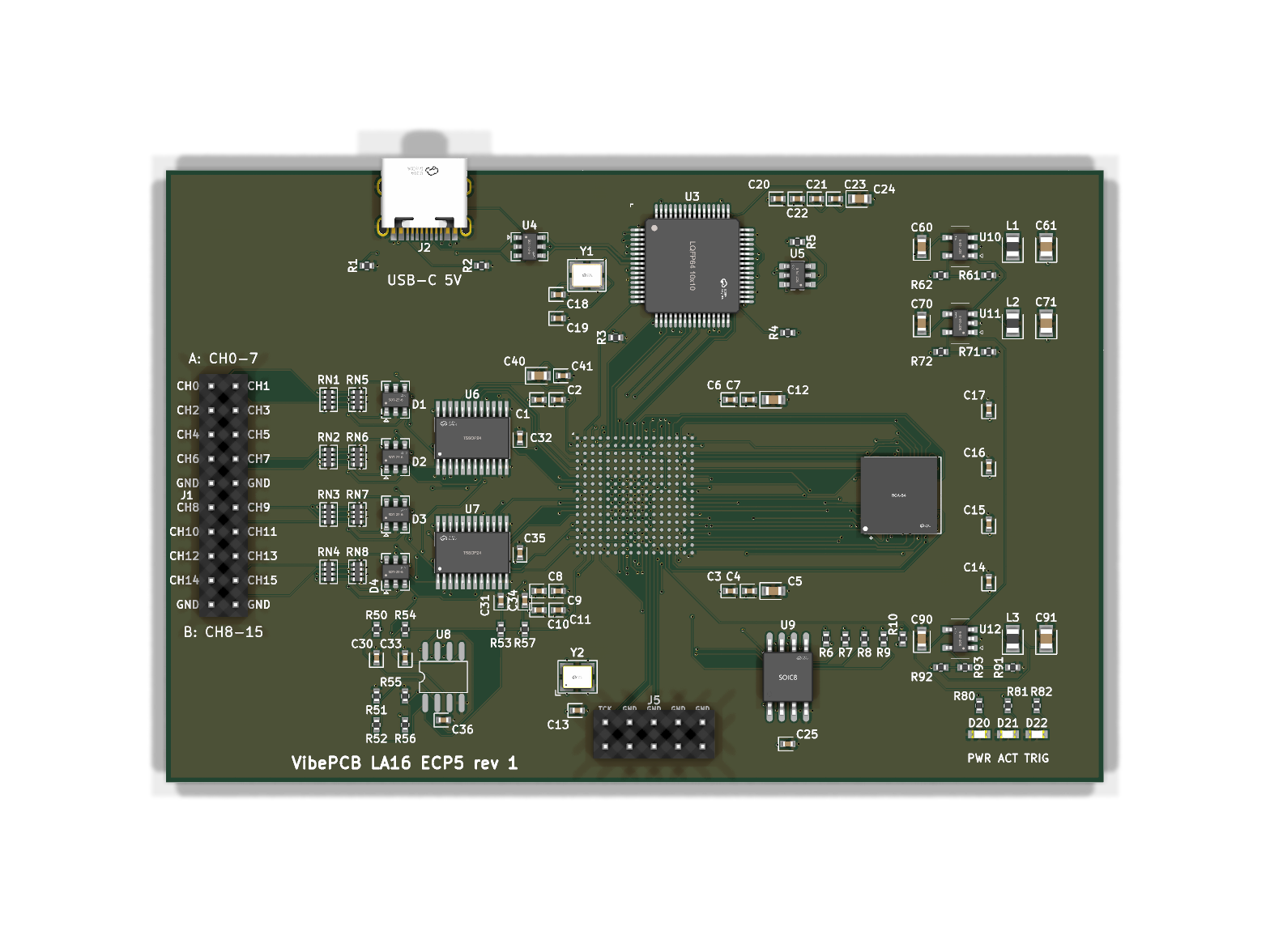
A 16-channel, 100 MSa/s USB 2.0 HS logic analyzer: a Lattice ECP5 FPGA (CABGA-256 BGA) capturing into a 32 MB SDRAM (54-ball BGA), read out over an FT2232H. 98 x 64 mm, 6 layers.
La ecp5 is an open-source printed circuit board by PaulBichl, from the PaulBichl/VibePCB-LA repository on GitHub. It is a 6-layer board of 98 × 64 mm with 103 parts on 161 nets, routed with 1,487 tracks and 460 vias.
It is built around the LFE5U-25F-7BG256I, TLV62569DBVR-TP and FT2232HL-REEL, with the TLV9062IDR-MS, W25Q128JVSIQ and SN74LVC8T245PWRE4 among its other parts. Its parts include 40 capacitors, 28 resistors, 12 ICs, 7 diodes and 3 connectors. It belongs with the fPGA and programmable logic boards and the FPGA and CPLD boards of this library.


A 16-channel, 100 MSa/s USB 2.0 HS logic analyzer: a Lattice ECP5 FPGA (CABGA-256 BGA) capturing into a 32 MB SDRAM (54-ball BGA), read out over an FT2232H. 98 x 64 mm, 6 layers. Designed with VibePCB (tscircuit -> KiCad) as a stretch of the tooling: two 0.8 mm BGAs escaped and routed by VibePCB's own router, a length-checked 39-signal memory bus, a coupled 90 ohm USB pair, three power planes.
Status: passes check (KiCad DRC and ERC with 0 errors, house rules). Not fabricated yet.
| Schematic | |
| Layout | PDF, one page per copper layer, front, back |
| 3D | top, bottom |
| BOM (LCSC / MPN) | CSV |
| KiCad project | kicad/ |
| Source | index.circuit.tsx (tscircuit), vibepcb.toml (rules, planes, length groups, BGA escape), routes.toml (routing order) |
The KiCad project opens as it is. The 3D models are left out because they are tens of MB;
pcb fix downloads them. Gerbers and pick-and-place files are not in the repo: either plot them
from the KiCad project, or build the board (below) and run hatch run pcb fab la-ecp5, which
writes Gerbers, drill, BOM, CPL and a JLCPCB upload set.
| Channels | 16, two banks of 8, threshold per bank (I/O rail 1.2-5 V, threshold ~ rail / 2) |
| Sample rate | 100 MSa/s x 16 into SDRAM |
| Buffer | 32 MB (256 Mbit 16-bit SDR SDRAM) = 16 M samples x 16 ch |
| Streaming | ~40 MB/s over USB 2.0 HS (FT2232H sync FIFO): 16 ch at ~20 MSa/s |
| Inputs | 1 Mohm, 1k series + SRV05-4 clamps to the bank rail / GND |
| Probe | 2x10 2.54 mm header (16 signals + 4 GND), labelled per pin |
| Power | USB-C 5 V, < 3 W |
| Debug | JTAG header (J5), 3 LEDs (power, activity, trigger) |
 probe     +--------------+    +---------------+    +-------------+
 header -->| 1k, 1M,      |--->| 74LVC8T245 x2 |--->|             |<--- 100 MHz osc
 16 ch     | SRV05-4      |    | level shift   |    |  ECP5-25F   |
           +--------------+    +---------------+    |  CABGA-256  |<==> IS42S16160J SDRAM
                  ^                    ^            |             |     (32 MB, BGA-54)
                  +--- bank rail ------+            |             |
                       1.2-5 V, x2                  |             |<--- JTAG (J5)
                          ^                         |             |
               TLV9062 + RC filter <------ PWM -----|             |
                                                    +--+-------+--+
                                                       ^       ^
                                    W25Q128 -----------+       | 8-bit sync FIFO
                                    config flash               v
                                       ^  SPI (ch B)     +---------+  USB 2.0 HS  +------------+
                                       +-----------------| FT2232H |<============>| USB-C, ESD |
                                                         +---------+              +-----+------+
                                                                                        | 5 V
                                           3.3 V, 1.1 V, 2.5 V <--- TLV62569 x3 <-------+
Signal path. A probe signal enters the 2x10 header, passes a 1k series resistor (with the SRV05-4 clamping it to the bank rail and GND, and 1M pulling an open input low) and reaches a 74LVC8T245. Its A side runs on the bank rail, so the input threshold follows that rail (~ rail / 2); its B side runs on 3.3 V and drives the FPGA. One translator per bank of 8 channels, so two target logic families can be probed at once.
Threshold. The FPGA sets each bank rail itself: a PWM pin, a 10k / 1 uF RC filter, a TLV9062 op-amp with gain 1.5 -> 1.2 to 4.95 V. No DAC chip needed.
Capture. The FPGA samples all 16 inputs at 100 MHz (from the oscillator on a primary clock input), runs the trigger logic and writes the samples to the SDRAM: 16 bit x 100 MSa/s = 200 MB/s, which the 16-bit SDRAM (-7 grade, rated to 143 MHz) takes in bursts; 32 MB = 16 M samples (0.16 s at full rate).
Readout. The FT2232H is the USB 2.0 high-speed interface: channel A is an 8-bit synchronous FIFO to the FPGA (~40 MB/s, its 60 MHz CLKOUT on a primary clock input), enough to read the buffer out or to stream 16 ch at ~20 MSa/s live. Channel B (MPSSE) writes the FPGA bitstream into the W25Q128 SPI flash while it holds PROGRAMN low; the FPGA boots from it in master SPI mode (CFG[2:0] = 010), so no separate programmer is needed. The 93LC56 EEPROM stores the FT2232H's FIFO-mode setting.
Power. USB-C 5 V (5.1k CC pull-downs, no PD) -> three TLV62569 bucks: 3.3 V for I/O, SDRAM and USB, 1.1 V for the FPGA core, 2.5 V for its aux supply. Under 3 W.
Why this FPGA. The ECP5 LFE5U-25F has 24k LUTs, 1 Mbit of block RAM and plenty of I/O for 16 inputs + the 39-signal SDRAM bus + the FIFO, with a fully open toolchain (yosys / nextpnr-ecp5 / Project Trellis). Its block RAM alone would only hold ~60 k samples, hence the SDRAM. The CABGA-256 package was the point of the exercise: an earlier version of this board used an iCE40HX4K in a TQFP-144 (4 layers, in git history) because tscircuit's router could not escape a BGA; VibePCB now does the escape and routing itself.
Net classes, the USB pair, the length groups, the planes and the escape settings live in
boards/la-ecp5/vibepcb.toml; the routing order in
routes.toml.
| Part | LCSC |
|---|---|
| LFE5U-25F-7BG256I (FPGA) | C1550762 |
| IS42S16160J-7BLI (SDRAM) | C1348766 |
| FT2232HL (USB) | C27882 |
| SN74LVC8T245PWR | C27643 |
| W25Q128JVSIQ (config flash) | C97521 |
| 93LC56BT-I/OT | C190271 |
| SX3M100.000B20F30TNN (100 MHz osc) | C5179979 |
| X322512MSB4SI (12 MHz crystal) | C9002 |
| TLV62569DBVR | C141836 |
| TLV9062IDR | C398355 |
| USBLC6-2SC6 | C7519 |
| SRV05-4 | C2836319 |
| TYPE-C-31-M-12 | C165948 |
Passives are in the BOM. Check stock before ordering.
Clone vibepcb next to this repo as VibePCB, then
hatch run setup
hatch run pcb all la-ecp5       # build, fix, route, check
hatch run pcb publish la-ecp5   # refresh boards/la-ecp5/hardware/
hatch run pcb fab la-ecp5       # Gerbers, drill, BOM, CPL
package.json pins the tscircuit version the board was built with, because routing differs
between versions.
Out of scope for this repo: FPGA gateware and the host software (a sigrok driver).
| Qty | Value | Footprint | References |
|---|---|---|---|
| 24 | 100nF | tscircuit:capacitor_cap0402 | C1, C2, C3, C10, C11, C13, C14, C15, C16, C17, C20, C21, C22, C23, C25, C32 +8 |
| 13 | 10kΩ | tscircuit:resistor_res0402 | R4, R6, R7, R8, R9, R10, R50, R51, R54, R55, R72, R91, R93 |
| 6 | 10uF | tscircuit:capacitor_cap0603 | C5, C12, C40, C60, C70, C90 |
| 4 | 1uF | tscircuit:capacitor_cap0402 | C30, C31, C33, C34 |
| 4 | 4D02WGJ0102TCE | tscircuit:4D02WGJ0102TCE | RN1, RN2, RN3, RN4 |
| 4 | RTA02-4D105JTH | tscircuit:RTA02-4D105JTH | RN5, RN6, RN7, RN8 |
| 4 | SRV05-4 | tscircuit:SRV05-4 | D1, D2, D3, D4 |
| 3 | 2.2µH | tscircuit:inductor_0805 | L1, L2, L3 |
| 3 | 22uF | tscircuit:capacitor_cap0805 | C61, C71, C91 |
| 3 | 330Ω | tscircuit:resistor_res0402 | R80, R81, R82 |
| 3 | KT-0603G | tscircuit:KT-0603G | D20, D21, D22 |
| 3 | TLV62569DBVR | tscircuit:TLV62569DBVR | U10, U11, U12 |
| 2 | 10Ω | tscircuit:resistor_res0402 | R53, R57 |
| 2 | 12kΩ | tscircuit:resistor_res0402 | R3, R71 |
| 2 | 18pF | tscircuit:capacitor_cap0402 | C18, C19 |
| 2 | 20kΩ | tscircuit:resistor_res0402 | R52, R56 |
| 2 | 22kΩ | tscircuit:resistor_res0402 | R61, R92 |
| 2 | 5.1kΩ | tscircuit:resistor_res0402 | R1, R2 |
| 2 | SN74LVC8T245PWR | tscircuit:SN74LVC8T245PWR | U6, U7 |
| 1 | 100kΩ | tscircuit:resistor_res0402 | R62 |
| 1 | 2.2kΩ | tscircuit:resistor_res0402 | R5 |
| 1 | 4.7uF | tscircuit:capacitor_cap0603 | C24 |
| 1 | 93LC56BT-I/OT | tscircuit:93LC56BT-I_OT | U5 |
| 1 | FT2232HL-REEL | tscircuit:FT2232HL-REEL | U3 |
| 1 | IS42S16160J-7BLI | tscircuit:IS42S16160J-7BLI | U2 |
| 1 | LFE5U-25F-7BG256I | tscircuit:LFE5U-25F-7BG256I | U1 |
| 1 | SX3M100.000B20F30TNN | tscircuit:SX3M100_000B20F30TNN | Y2 |
| 1 | TLV9062IDR | tscircuit:TLV9062IDR | U8 |
| 1 | TYPE-C-31-M-12 | tscircuit:TYPE-C-31-M-12 | J2 |
| 1 | USBLC6-2SC6 | tscircuit:USBLC6-2SC6 | U4 |
| 1 | W25Q128JVSIQ | tscircuit:W25Q128JVSIQ | U9 |
| 1 | X322512MSB4SI | tscircuit:X322512MSB4SI | Y1 |
| 1 | pin_header_pinrow10_p2_54_rows2 | tscircuit:pin_header_pinrow10_p2_54_rows2 | J5 |
| 1 | pin_header_pinrow20_p2_54_nopinlabels_rows2 | tscircuit:pin_header_pinrow20_p2_54_nopinlabels_rows2 | J1 |
embeddedos-org/eCAD-Hardware-Products
Hardware designs + EE docs + Board datasheets of Multiple products

jayis1/hacker-devices
Full-cycle hardware designs for security research devices — each device is a subfolder with its own README, schematics, PCB layout, and software stack

kocer/direct-sampling-sdr
Direct-sampling SDR transceiver with four phase-coherent channels, and a class-A power amplifier for 1.8 to 54 MHz.


It measures 98 × 64 mm and has 6 copper layers, 1.6 mm thick.
103 parts, built around the LFE5U-25F-7BG256I, TLV62569DBVR-TP, FT2232HL-REEL and TLV9062IDR-MS. The full list of its parts is on this page, with links to each part's symbol and footprint where PCBKit's library has them.
From the PaulBichl/VibePCB-LA repository on GitHub, at the commit this page was made from: the board is boards/la-ecp5/hardware/kicad/la-ecp5.kicad_pcb and its schematic boards/la-ecp5/hardware/kicad/la-ecp5.kicad_sch. PCBKit opens the board in the browser, with nothing to install.
Its repository states no licence, so its author keeps all rights: ask PaulBichl before reusing the design.