Skip to the content
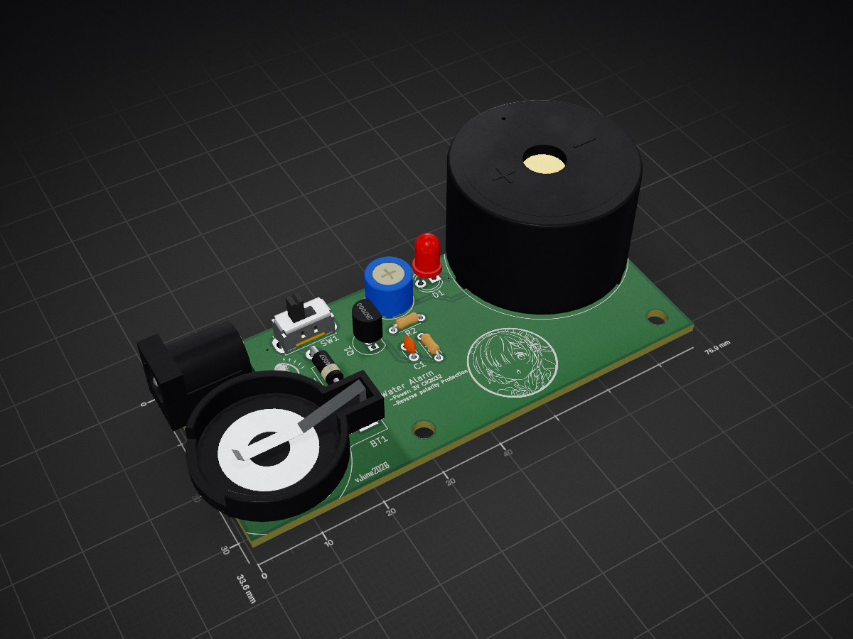
2 layers76.9 × 33.6 mmWater alarm Project, the printed circuit board in 3D

Water alarm Project

Parampreet39/Learning-KiCad

This repository documents my transition from "scrap" electronics to professional Monozukuri (craftsmanship). It contains my schematics, board layouts, and project evolution as I master the art of PCB design for IoT and…

Size
76.9 × 33.6 mm
Copper layers
2
Thickness
1.6 mm
Parts
15
Nets
9
Pads
29
Tracks, vias
43, 2
Pours
2
Routed
Yes
KiCad
KiCad 10.0 (file 20260206)
Created
17 May 2026
Updated
26 Jun 2026

Overview

Water alarm Project is an open-source printed circuit board by Parampreet39, from the Parampreet39/Learning-KiCad repository on GitHub. It is a 2-layer board of 76.9 × 33.6 mm with 15 parts on 9 nets, routed with 43 tracks and 2 vias.

Its parts include 2 resistors, 2 diodes, 1 capacitor, 1 transistor and 1 connector.

README

README.md

⚡ Learning KiCad: Hardware & PCB Design

This repository documents my transition from "scrap" electronics to professional Monozukuri (craftsmanship). It contains my schematics, board layouts, and project evolution as I master the art of PCB design for IoT and Audio applications.


🏆 Featured Project: 5V to 3.3V Linear Regulator

My first complete PCB design focused on stable power delivery for microcontrollers.

✅ Key Features & Skills Demonstrated:

  • Schematic Capture: Proper use of decoupling capacitors and power symbols.
  • Physical Layout: Managed footprints for SMD (AMS1117-3.3) and Through-Hole components.
  • Thermal Management: Implemented Via Stitching to dissipate heat between copper layers.
  • Signal Integrity: Designed Copper Pours (Ground Zones) on both layers to minimize electrical noise.
  • Design Rule Check (DRC): Optimized the layout to achieve Zero Violations and Zero Unconnected Items.
  • Branding: Custom silkscreen art and QR code integration for documentation.

🛠️ The Roadmap

  1. Basics: Water Alarm image image V2 Modified it
    • Added : Cell Input , Diode for Reverse polarity protection , Potentiometer for Volume Change image
    image

Designed by: Parampreet39 | Target: Mechanical Engineering & IoT

Parts

15
QtyValueFootprintReferences
2LOGOLOGOG***, G***
110MResistor_THT:R_Axial_DIN0204_L3.6mm_D1.6mm_P5.08mm_HorizontalR1
11N4007Diode_THT:D_DO-41_SOD81_P10.16mm_HorizontalD2
11kPotentiometer_THT:Potentiometer_Bourns_3339P_Vertical_HandSolderingRV1
11nfCapacitor_THT:C_Disc_D3.0mm_W1.6mm_P2.50mmC1
1200Resistor_THT:R_Axial_DIN0204_L3.6mm_D1.6mm_P5.08mm_HorizontalR2
12N7000Package_TO_SOT_THT:TO-92_InlineQ1
1Battery_CellBattery:BatteryHolder_Keystone_103_1x20mmBT1
1BuzzerBuzzers:Buzzer_D30mm_H20mm_P15mm__668-1652-ND__AI-3035-TT-12V-RBZ1
1Jack-DCConnector_BarrelJack:BarrelJack_GCT_DCJ200-10-A_HorizontalJ1
1LED_Small_FilledLED_THT:LED_D4.0mmD1
1SW_SPDTButton_Switch_THT:SW_Slide_SPDT_Straight_CK_OS102011MS2QSW1

The 13 most common of 15 parts.

More from Parampreet39/Learning-KiCad

1
  • 2 layers59.1 × 26.8 mmVoltage, the printed circuit board in 3D

    Voltage

    Parampreet39/Learning-KiCad

    This repository documents my transition from "scrap" electronics to professional Monozukuri (craftsmanship). It contains my schematics, board layouts, and project evolution as I master the art of PCB design for IoT and…

    8 parts

Similar boards

  • 2 layers19 × 76 mmSub, the printed circuit board in 3D

    Sub

    google/mozc-devices

    Circuit diagrams and firmware source code for Gboard DIY keyboards

    15 parts3kApache-2.0
  • 2 layers26.7 × 62.2 mmDeniseadapter, the printed circuit board in 3D

    Deniseadapter

    hoglet67/RGBtoHDMI

    Bare-metal Raspberry Pi project that provides pixel-perfect sampling of Retro Computer RGB/YUV video and conversion to HDMI

    15 parts1kGPL-3.0
  • 2 layers100 × 44 mmVideoslot, the printed circuit board in 3D

    Videoslot

    mntmn/amiga2000-gfxcard

    MNT VA2000, an Open Source Amiga 2/3/4000 Graphics Card (Zorro II/III), written in Verilog

    15 parts1k
  • 2 layers91 × 51 mmBusinessCard, the printed circuit board in 3D

    BusinessCard

    hackclub/OnBoard

    💡 Join 1,000 teenagers and make your first PCB with a $100 grant!

    15 parts915
  • 2 layers24.3 × 57.9 mmFlosspods pro flex, the printed circuit board in 3D

    Flosspods pro flex

    kenp-io/not-for-airpods-repairs

    The content of this repository is licensed under the WTFPL License. Please have a close look at the terms before using this material.

    15 parts609WTFPL
  • 2 layers20.3 × 15.2 mmL0 Load, the printed circuit board in 3D

    L0 Load

    Luos-io/luos_engine

    Open-source and real-time orchestrator for cyber-physical-systems, to easily design, test and deploy embedded applications and digital twins.

    15 parts546MIT
  • 2 layers68 × 50 mmEleLab v2 PowerFeed, the printed circuit board in 3D

    EleLab v2 PowerFeed

    Chrismettal/EleLab_v2

    Cheap DIY lab system for hobbyists and the tinkering folk

    15 parts531GPL-3.0
  • 2 layers50.8 × 35.6 mmInterface, the printed circuit board in 3D

    Interface

    harbaum/I2C-Tiny-USB

    Cheap and simple I²C to USB interface

    15 parts454

Questions

How big is the Water alarm Project PCB?

It measures 76.9 × 33.6 mm and has 2 copper layers, 1.6 mm thick.

What parts does the Water alarm Project use?

15 parts. The full list of its parts is on this page, with links to each part's symbol and footprint where PCBKit's library has them.

Where can I download the Water alarm Project KiCad files?

From the Parampreet39/Learning-KiCad repository on GitHub, at the commit this page was made from: the board is Water alarm Project/Water alarm Project.kicad_pcb and its schematic RGB matrix/RGB matrix.kicad_sch. PCBKit opens the board in the browser, with nothing to install.

Can I use the Water alarm Project design in my own project?

Its repository states no licence, so its author keeps all rights: ask Parampreet39 before reusing the design.