
2 layers85.4 × 54.1 mm

 NoseFa/Fallout-NFC-Badge
An NFC badge made for Hack Club Fallout. This project was done on the first full day of Hack Club Fallout as a PCB sprint project. We had around like 7-8h from start to finish.
FalloutPCBs is an open-source printed circuit board by NoseFa, from the NoseFa/Fallout-NFC-Badge repository on GitHub. It is a 2-layer board of 92 × 51 mm with 11 parts on 8 nets, routed with 41 tracks and 3 vias.
It is built around the NT3H2111W0FHKH. Its parts include 1 capacitor, 1 resistor, 1 IC and 1 diode.
An NFC badge made for Hack Club Fallout. This project was done on the first full day of Hack Club Fallout as a PCB sprint project. We had around like 7-8h from start to finish. The badge was made to fit the holders / landyards given to us at the event. The badge includes an nfc tag and a whitescreen with a QR code to the fallout home page and a code to my github profile on the back side. I will probably program the nfc tag to forward to the photo site so I can quickly give people access to it. This was also one of my first KiCad projects with PCBA components so it's pretty bare bones and simple.
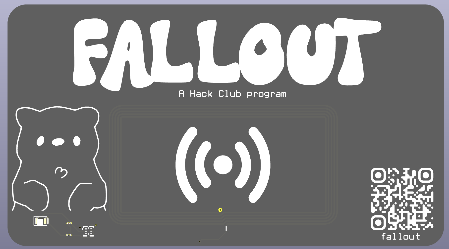
Front side with the NFC tag area, Fallout logo, soup (Fallout's mascot) and a QR code to the Fallout page.
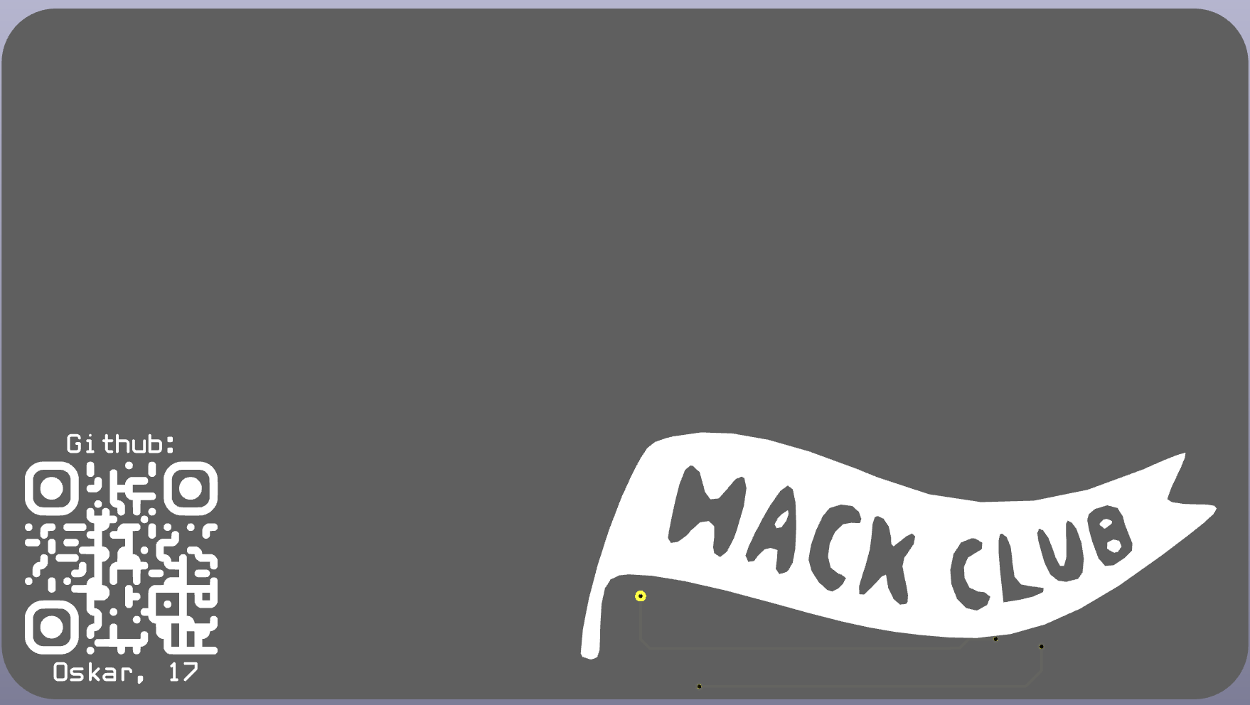
Back side with the Hack Club flag and QR code to my GitHub
I made this project in KiCad and got it manufactured by JLCPCB as a PCBA. When ordering keep in mind that the antenna might be listed as a part but it doesn't need to be placed so when it gives an error for the antenna not having a part mapped to it in the BOM thats normal. You can find the manufacturing files in kicad/jlcpcb/production_files. It includes the gerbers and the BOM.
| Qty | Value | Footprint | References |
|---|---|---|---|
| 6 | LOGO | LOGO | G***, G***, G***, G***, G***, G*** |
| 1 | Antenna_Loop | kicad_why:25X48MM_NFC | AE1 |
| 1 | C | Capacitor_SMD:C_0201_0603Metric | C1 |
| 1 | LED | LED_SMD:LED_0805_2012Metric | D1 |
| 1 | NT3H2111W0FHKH | kicad_why:XQFN-8_L1.6-W1.6-P0.50-BL_NT3H2111W0FHKH | U1 |
| 1 | R | Resistor_SMD:R_0201_0603Metric | R1 |


nushackers/hnr26-badge-quacknroll
Hack&Roll 2026 "Quack & Roll" badge source files, for both hardware and firmware


ElectronicCats/badge-dragonJar-2025
¡El badge oficial de DragonJarCON 2025! Un dispositivo NFC programable con pantalla OLED, múltiples LEDs y un reto de hacking integrado. Diseñado para la comunidad de DragonJar


It measures 92 × 51 mm and has 2 copper layers, 1.6 mm thick.
11 parts, built around the NT3H2111W0FHKH. The full list of its parts is on this page, with links to each part's symbol and footprint where PCBKit's library has them.
From the NoseFa/Fallout-NFC-Badge repository on GitHub, at the commit this page was made from: the board is FalloutPCBs.kicad_pcb and its schematic FalloutPCBs.kicad_sch. PCBKit opens the board in the browser, with nothing to install.
Its repository states no licence, so its author keeps all rights: ask NoseFa before reusing the design.