2 layers98 × 27 mm
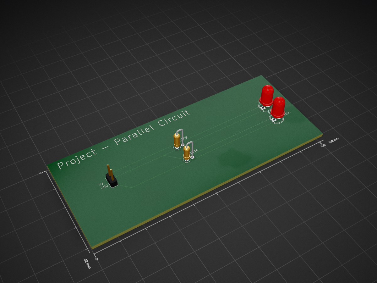
 Nikolov999/Project-Parallel-Circuit
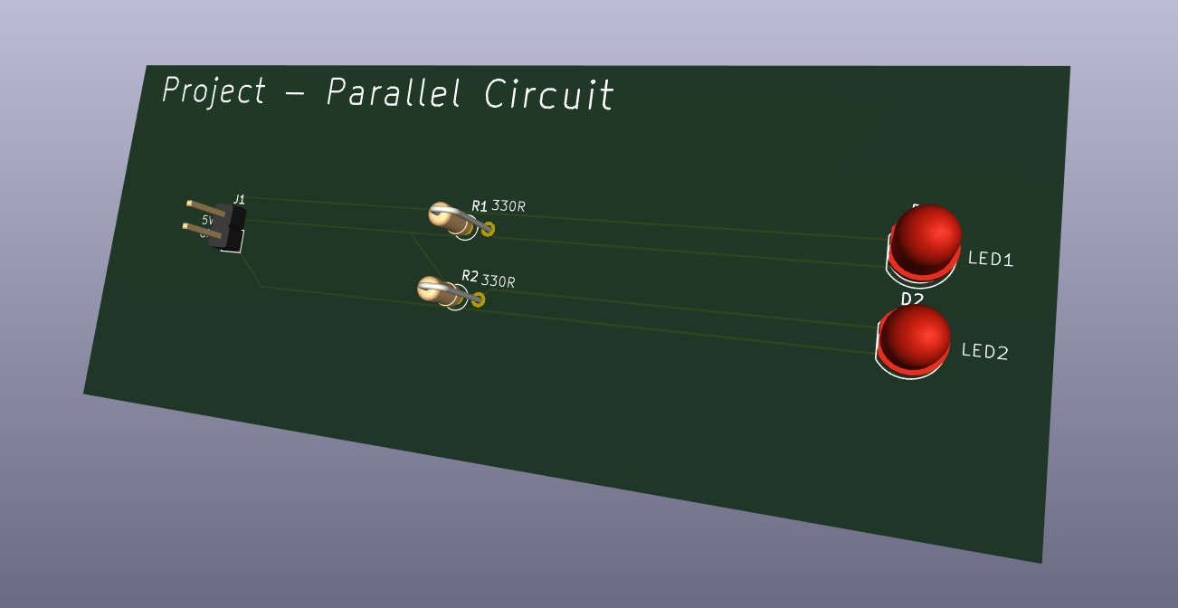
Created my first parallel circuit with dual LEDs.
Project Parallel Circuit is an open-source printed circuit board by Nikolov999, from the Nikolov999/Project-Parallel-Circuit repository on GitHub. It is a 2-layer board of 102 × 42 mm with 5 parts on 4 nets, routed with 20 tracks and 0 vias.
Its parts include 2 resistors, 2 diodes and 1 connector.
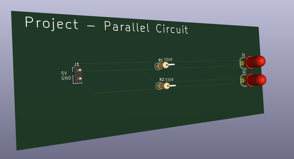
A first hands-on KiCad PCB project built to explore a real parallel DC circuit from electrical calculation through schematic capture, footprint assignment, PCB layout, routing, verification, and 3D inspection.
The board uses a 5 V input and two independent LED branches. Each branch contains its own 330 Ω current-limiting resistor and LED, so the resistor/LED pair is series-connected inside the branch while the two complete branches are connected in parallel.
                     Branch 1
              R1 330 Ω        D1
          +---/\/\/\/---------|>|---+
          |                         |
+5 V -----+                         +----- GND
          |                         |
          +---/\/\/\/---------|>|---+
              R2 330 Ω        D2
                     Branch 2
Electrical structure:
Design assumptions:
Vs = 5 VVf = 2 VVoltage across each resistor:
Vr = Vs - Vf
Vr = 5 V - 2 V
Vr = 3 V
Approximate branch current:
I = Vr / R
I = 3 V / 330 Ω
I ≈ 0.00909 A
I ≈ 9.1 mA
Because the branches are parallel and use the same nominal component values:
I1 ≈ 9.1 mA
I2 ≈ 9.1 mA
Itotal = I1 + I2
Itotal ≈ 18.2 mA
Approximate resistor dissipation:
P = Vr × I
P ≈ 3 V × 0.00909 A
P ≈ 0.027 W
A 0.25 W resistor rating therefore provides substantial margin for the assumed operating point.
Vf = 2 Vis a design approximation. Real LED forward voltage varies with LED type, colour, current, temperature, and manufacturing tolerance, so measured current will differ somewhat from the calculated value.
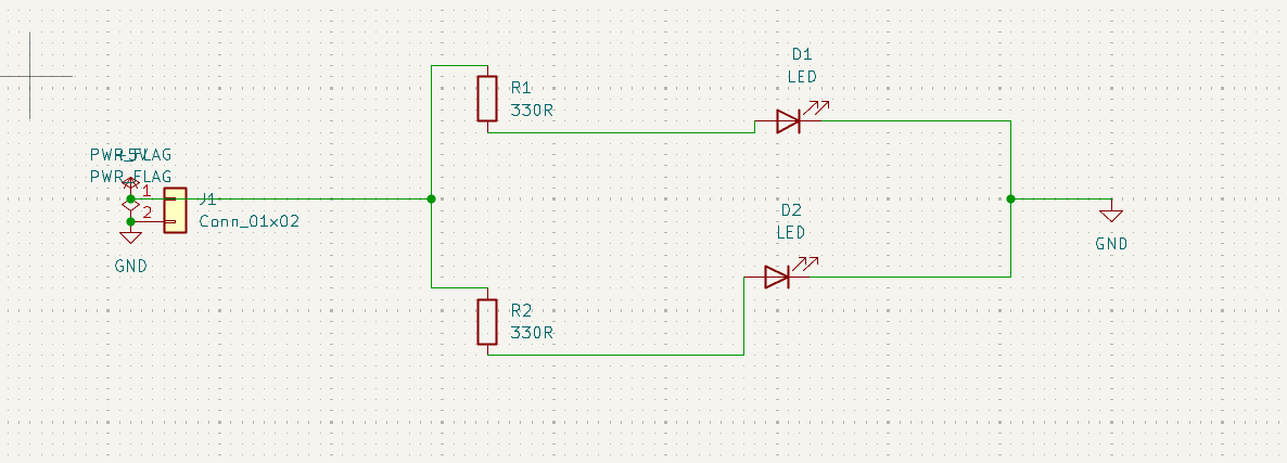
The schematic was built with two independent current-limited LED branches tied between the same +5 V and GND nodes. Power flags are used so KiCad's electrical rules checker understands that the rails are driven from an external source through J1.
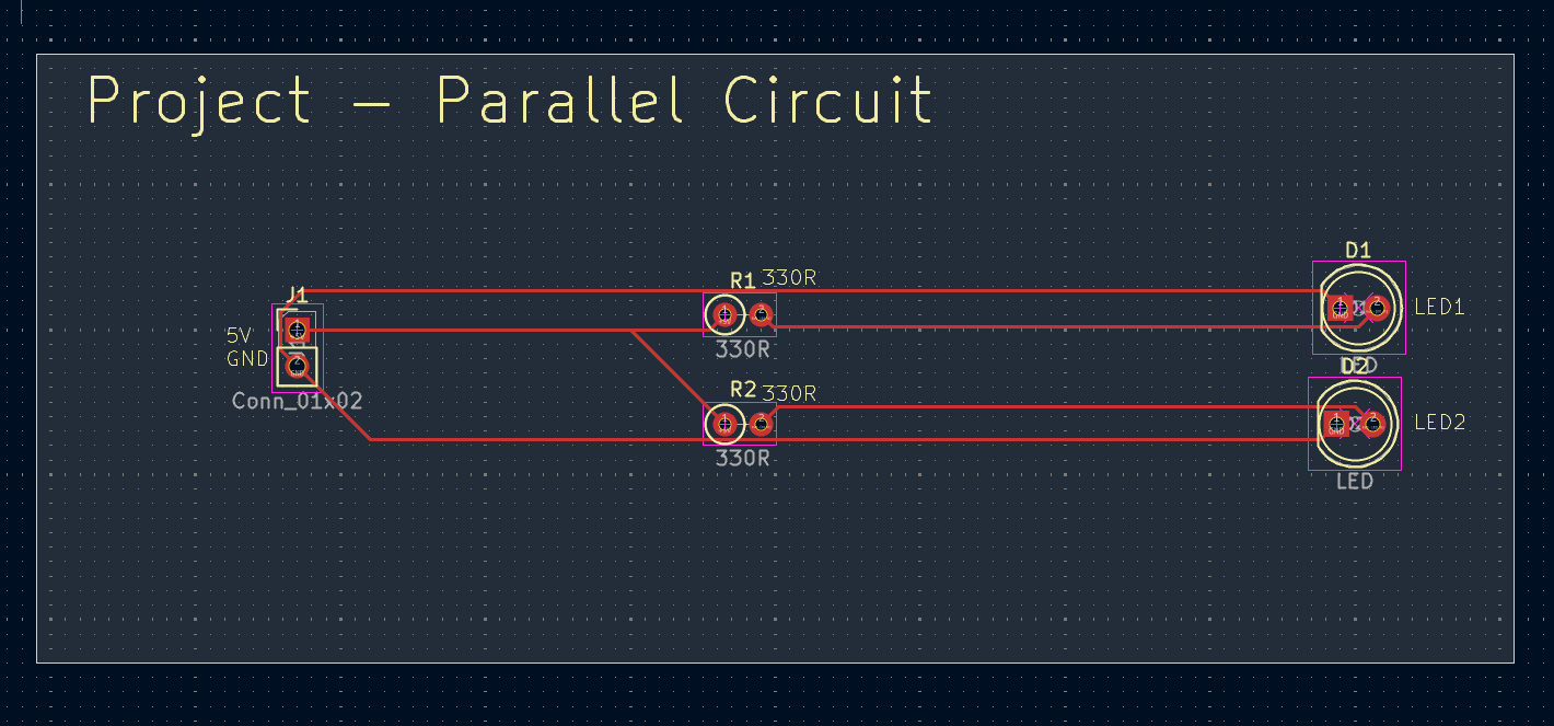
The board is intentionally spacious so the two branches are visually obvious. The current revision uses:
| Reference | Qty | Value / Part | Footprint |
|---|---|---|---|
| J1 | 1 | 1×02 connector | PinHeader_1x02_P2.54mm_Vertical |
| R1, R2 | 2 | 330 Ω resistor | R_Axial_DIN0207_L6.3mm_D2.5mm_P2.54mm_Vertical |
| D1, D2 | 2 | 5 mm LED | LED_D5.0mm |
A machine-readable version is available in BOM.csv.
Final checks completed in KiCad:
Project-Parallel-Circuit/
├── README.md
├── BOM.csv
├── .gitignore
├── .gitattributes
├── kicad/
│   ├── Project-Parallel-Circuit.kicad_pro
│   ├── Project-Parallel-Circuit.kicad_sch
│   └── Project-Parallel-Circuit.kicad_pcb
├── docs/
│   ├── board-definition.md
│   ├── calculations.md
│   ├── design-notes.md
│   └── source-notes/
│       ├── Board-Definition-original.txt
│       └── Calculating-Branches-original.txt
├── images/
│   ├── schematic.png
│   ├── pcb-layout.png
│   ├── pcb-3d-front.png
│   └── pcb-3d-angle.png
└── fabrication/
    ├── README.md
├── Project-Parallel-Circuit-Gerbers.zipEdge.CutsDesigned with KiCad 10.
The repository includes the final Gerber job, separate manufacturing layers, plated/non-plated Excellon drill files, and a ready-to-upload manufacturing ZIP. The corrected export keeps Plot on All Layers empty so copper and silkscreen are not duplicated into unrelated manufacturing layers.
Basic checks performed on this export:
Edge_Cuts contains only the closed 102 mm × 42 mm board profile.F.Cu contains the front routing and through-hole pads.B.Cu contains through-hole pad copper without copied front routing.Project-Parallel-Circuit-PTH.drl contains 10 plated component holes.Project-Parallel-Circuit-NPTH.drl is empty because the board has no NPTH mechanical holes.See fabrication/README.md for the file set.
| Qty | Value | Footprint | References |
|---|---|---|---|
| 2 | 330R | Resistor_THT:R_Axial_DIN0207_L6.3mm_D2.5mm_P2.54mm_Vertical | R1, R2 |
| 2 | LED | LED_THT:LED_D5.0mm | D1, D2 |
| 1 | Conn_01x02 | Connector_PinHeader_2.54mm:PinHeader_1x02_P2.54mm_Vertical | J1 |

joypad-ai/joypad-os
Universal controller firmware for building adapters, dongles, and custom controllers.

OLIMEX/OLINUXINO
OLINUXINO is Open Source / Open Hardware, low cost from EUR 24 Linux Industrial grade Single Board Computer capable to operate -25+85C

jamro/tiny-engineer
A small desktop robot that brings an AI coding assistant to life, physically acting out when it reads files, thinks, writes code, and finishes work.

hackclub/OnBoard
💡 Join 1,000 teenagers and make your first PCB with a $100 grant!


Luos-io/luos_engine
Open-source and real-time orchestrator for cyber-physical-systems, to easily design, test and deploy embedded applications and digital twins.
It measures 102 × 42 mm and has 2 copper layers, 1.6 mm thick.
5 parts. The full list of its parts is on this page, with links to each part's symbol and footprint where PCBKit's library has them.
From the Nikolov999/Project-Parallel-Circuit repository on GitHub, at the commit this page was made from: the board is kicad/Project-Parallel-Circuit.kicad_pcb and its schematic kicad/Project-Parallel-Circuit.kicad_sch. PCBKit opens the board in the browser, with nothing to install.
Its repository states no licence, so its author keeps all rights: ask Nikolov999 before reusing the design.