4 layers54.4 × 17.8 mm
29F160 to 27C322 2-0
MouseBiteLabs/ROM-Adapter-Boards
A collection of ROM adapter boards for different use cases
17 parts23CC-BY-SA-4.0
 MouseBiteLabs/ROM-Adapter-Boards23
A collection of ROM adapter boards for different use cases
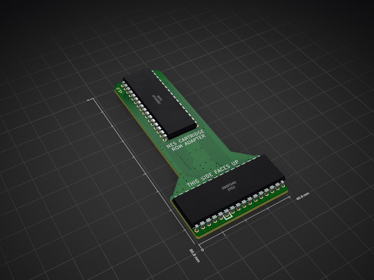
NES PRG CHR Combo Adapter 1-0 is an open-source printed circuit board by MouseBiteLabs, from the MouseBiteLabs/ROM-Adapter-Boards repository on GitHub, published under the CC-BY-SA-4.0 licence. It is a 2-layer board of 40.6 × 86.6 mm with 20 parts on 48 nets, routed with 542 tracks and 140 vias.
Its parts include 8 resistors, 2 ICs and 1 capacitor. It belongs with the interfaces and adapters and retro computing and games boards of this library.
This board is used to recreate the old UV EPROMs 27C160 and 27C322 with brand new 29F160 EEPROMs. The UV EPROMs are typically only available to purchase used from places like AliExpress and eBay, and are known to occasionally arrive damaged or completely inoperable. The 29F160, however, is brand new NOR Flash manufactured by Alliance, for purchase at major electronics distributors.
Here is a link to the component on Mouser.
With one of these chips, you can make a replacement for the 27C160. With two, you can make a replacement for the 27C322. In fact, with the 29F160's /BYTE pin, you can even make an 8-bit bus version of the 27C322 which was only ever a feature of the 27C160.
(In this image, the board is set up as a drop-in replacement for the 27C322)
All gerbers and source files can be found in this repo, as this project is fully open source. Please read all instructions associated with this board before assembling.
The zipped folder contains all the gerber files for this board. You can generally choose whatever thickness you want, but I usually stick to at least 1.0mm. The surface finish can also be whatever you want, but I find ENIG easier to solder the small-pitch parts, personally. Also note that this is a four-layer board.
You can order this board on OSH Park, which is a great option if you only need a small quantity: https://oshpark.com/shared_projects/efulo1p1
Alternatively, you can use the zipped folder at any board fabricator you like. You may also buy the board from PCBWay using this link (NOT YET AVAILABLE) (disclosure: I receive 10% of the sale value to go towards future PCB orders of my own):

To make programming this board easier, I made this mouthful of an adapter board: the TSOP NOR Flash Programming Adapter for T48. It is untested (I haven't received them yet) but if it works, it will let you program both of the 29F160 chips on this breakout board without having to desolder them. You will still need the TSOP48 adapter because there's a proprietary EEPROM chip on there to communicate with the main programmer, but this makes it easier nonetheless.
Remember: this adapter is untested. I will update this repository after testing it.
Most of the configurations are self-explanatory or are described on the back of the board, but here's a breakdown.
Bridge this solder pad if you are only using one 29F160 chip to replicate a 27C160. Note that this pad is located underneath U4 - meaning you should not solder JP1 if you have U4 on the board. U4 is required if you are using two 29F160 chips.
This is a special three-way set of pads that sets the mode for the databus output. These sets of pads configures the 29F160's /BYTE pin, which tells the chip to output data in an 8-bit bus or a 16-bit bus. The 27C160 had the same pin feature (as pin 32) but the 27C322 was forced to output a 16-bit bus. The /BYTE pin(s) on U2 and U3 are connected to the middle-right pad. Solder a resistor between the top or bottom set of pads, or directly connect this pad to the left (labeled "P32") according to the following criteria:
NOTE: Instead of a solder blob for P32 connection, a zero-ohm resistor may be used instead. Do not use any resistance value other than zero ohms for R2 if connecting to P32.
R1 and R3 are pull-up resistors for /WE and /RP pins on the 29F160s. When in normal operation, these two pins need to be pulled to VCC to operate properly. The /BYTE pin, as described in the section above, needs to be pulled to VCC or GND through R2 (or controlled through pin 32 elsewhere on the main board this is connecting to). The /BYTE pin is connected to the hole on the right side, also labeled /BYTE.
These holes are for easy access for potential on-board programming (these are used by the aformentioned 29F160 to UV EPROM Programmming Adapter for the T48). If you are using this adapter board on one of my cartridges, there may be support for in-circuit programming through these pins. See the repository for the cartridge in question for more information.
| Reference | Value/Part Number | Package | Description | Source |
|---|---|---|---|---|
| C1 | 0.1uF | 0603 | Capacitor (MLCC) | https://mou.sr/3ENc15O |
| R1 | 100k | 0603 | Resistor | https://mou.sr/49bgMnu |
| R2 (*NOTE) | 100k | 0603 | Resistor | https://mou.sr/49bgMnu |
| R2 (*NOTE) | Zero ohms | 0603 | Resistor (Jumper) | https://mou.sr/4e1ABQg |
| R3 | 100k | 0603 | Resistor | https://mou.sr/49bgMnu |
| U2 | M29F160 | TSOP-48 | Flash EEPROM | https://mou.sr/3HIjb09 |
NOTE: As described above, R2 is zero ohms (or a short circuit) to the P32 pad if you are using this board as a drop-in replacement for 27C160.
| Reference | Value/Part Number | Package | Description | Source |
|---|---|---|---|---|
| C1 | 0.1uF | 0603 | Capacitor (MLCC) | https://mou.sr/3ENc15O |
| C2 | 0.1uF | 0603 | Capacitor (MLCC) | https://mou.sr/3ENc15O |
| R1 | 100k | 0603 | Resistor | https://mou.sr/49bgMnu |
| R2 | 100k | 0603 | Resistor | https://mou.sr/49bgMnu |
| R3 | 100k | 0603 | Resistor | https://mou.sr/49bgMnu |
| U2 | M29F160 | TSOP-48 | Flash EEPROM | https://mou.sr/3HIjb09 |
| U3 | M29F160 | TSOP-48 | Flash EEPROM | https://mou.sr/3HIjb09 |
| U4 | 74HCT139 | TSSOP-16 | Decoder | https://mou.sr/4eqzppn |

This work is licensed under a Creative Commons Attribution-ShareAlike 4.0 International License. You are able to copy and redistribute the material in any medium or format, as well as remix, transform, or build upon the material for any purpose (even commercial) - but you must give appropriate credit, provide a link to the license, and indicate if any changes were made.
©MouseBiteLabs 2025
| Qty | Value | Footprint | References |
|---|---|---|---|
| 8 | R | Bucketmouse:R_0603_1608Metric_Boxed_SHORTED_DASHED | R1, R2, R3, R4, R5, R6, R7, R8 |
| 7 | Jumper_3_Open | Bucketmouse:SJ_2 | SJ1, SJ2, SJ3, SJ5, SJ6, SJ8, SJ9 |
| 2 | 39SF040 | Bucketmouse:DIP-32_W15.24mm | U1, U3 |
| 2 | Jumper_2_Open | Bucketmouse:SJ | SJ4, SJ7 |
| 1 | 0.1uF | Bucketmouse:THT_SMT_0803 | C1 |
MouseBiteLabs/ROM-Adapter-Boards
A collection of ROM adapter boards for different use cases

MouseBiteLabs/ROM-Adapter-Boards
A collection of ROM adapter boards for different use cases

MouseBiteLabs/ROM-Adapter-Boards
A collection of ROM adapter boards for different use cases

MouseBiteLabs/ROM-Adapter-Boards
A collection of ROM adapter boards for different use cases

MouseBiteLabs/ROM-Adapter-Boards
A collection of ROM adapter boards for different use cases


atopile/atopile
Design circuit boards with code! ✨ Get software-like design reuse 🚀, validation, version control and collaboration in hardware; starting with electronics ⚡️

davidphilipbarr/Sweep
Sweep - a small promicro based keyboard inspired by the Ferris.

rusefi/rusefi
rusefi - GPL internal combustion engine control unit

hoglet67/RGBtoHDMI
Bare-metal Raspberry Pi project that provides pixel-perfect sampling of Retro Computer RGB/YUV video and conversion to HDMI

hackclub/OnBoard
💡 Join 1,000 teenagers and make your first PCB with a $100 grant!

FreeYourStream/freedeck-hardware
all the stuff you need to build your own FreeDeck
It measures 40.6 × 86.6 mm and has 2 copper layers, 1.6 mm thick.
20 parts. The full list of its parts is on this page, with links to each part's symbol and footprint where PCBKit's library has them.
From the MouseBiteLabs/ROM-Adapter-Boards repository on GitHub, at the commit this page was made from: the board is NES ROM Adapter/NES_PRG_CHR_Combo_Adapter_1-0.kicad_pcb and its schematic 29F160 to UV EPROM/29F160_to_27C322_2-0.kicad_sch. PCBKit opens the board in the browser, with nothing to install.
Its repository publishes it under the CC-BY-SA-4.0 licence: you may reuse it on that licence's terms (keep the author's notice, and for a copyleft licence share your changes alike).