4 layers45 × 100 mm

 MaizeShark/Nikon-NMEA-Pro
low-power GNSS logger and BLE remote shutter for Nikon cameras
Nikon GPS is an open-source printed circuit board by MaizeShark, from the MaizeShark/Nikon-NMEA-Pro repository on GitHub. It is a 4-layer board of 30 × 30 mm with 79 parts on 105 nets, routed with 744 tracks and 173 vias.
It is built around the BMD-340-A-R, LSM303AGR and MAX-M10S, with the TPS70933DBV, TXU0101 and USBLC6-2SC6 among its other parts. Its parts include 35 resistors, 19 capacitors, 9 ICs, 5 connectors and 4 transistors. It belongs with the radio and wireless boards of this library.


A low-power GNSS logger and BLE remote shutter for Nikon cameras with the 10-pin connector. It is a work in progress: the hardware is designed, the PCB has not been built or tested, and the firmware has not been started.
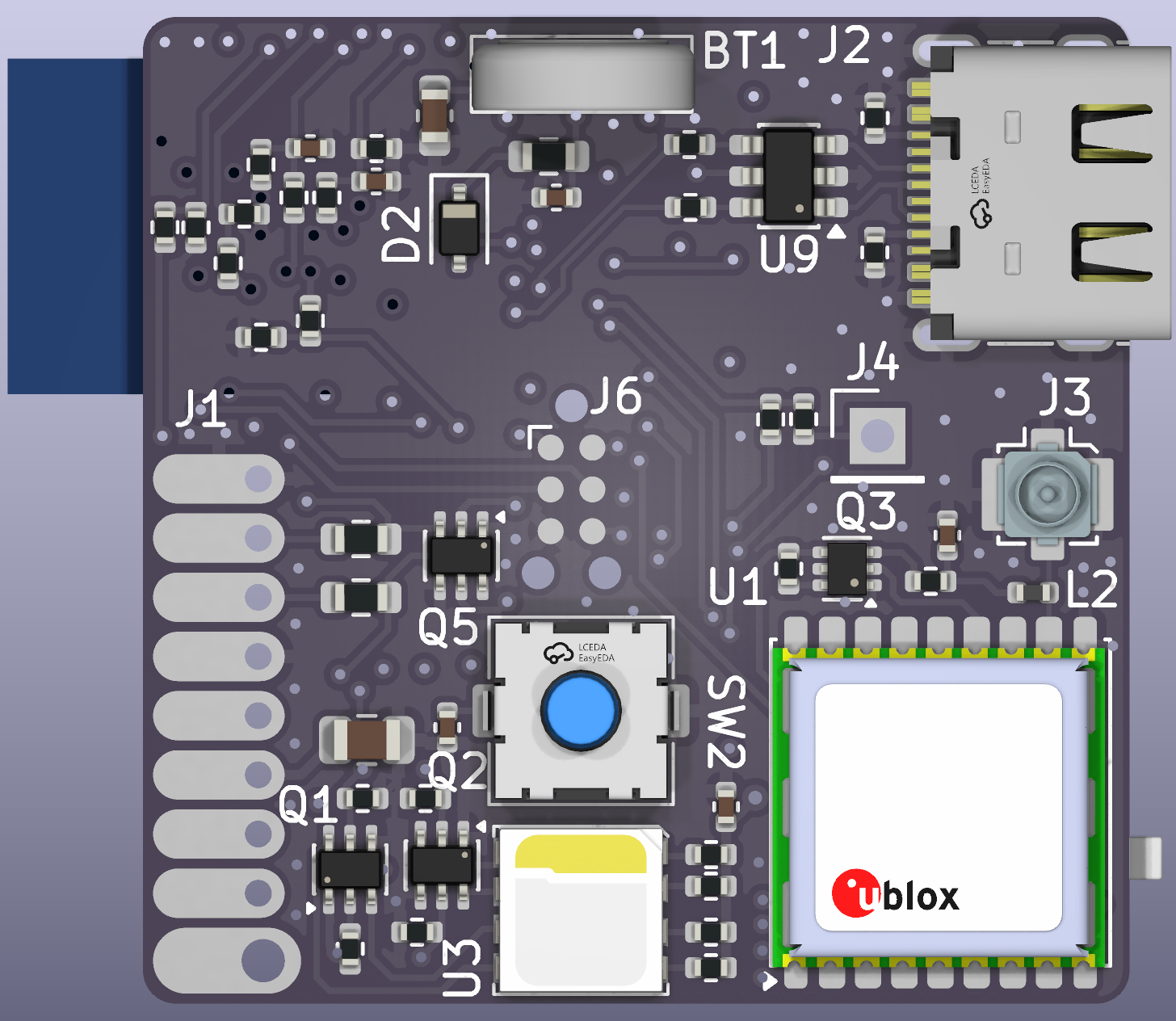
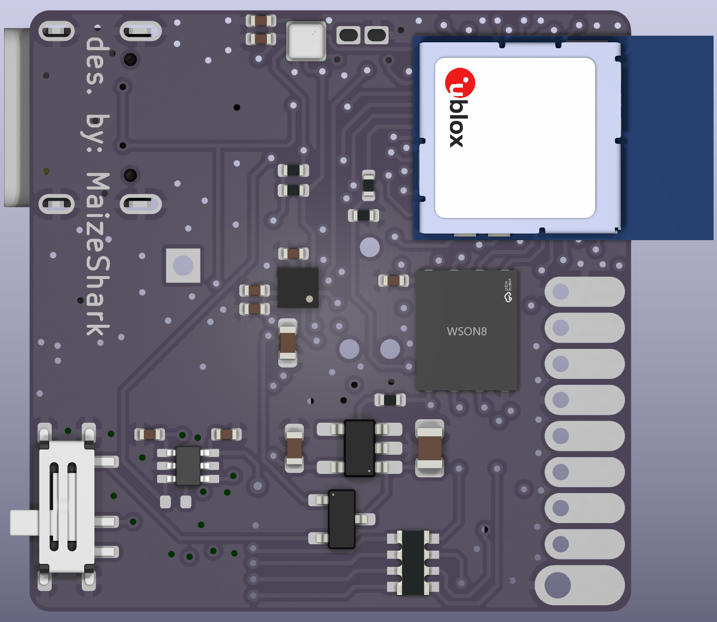
Front (left) and back (right) of the PCB.
Older GPS units for Nikon cameras (GP-1, Solmeta GMAX) typically draw tens of mA continuously, are slow to get a cold fix, and have no wireless connectivity. This 35 x 35 mm module aims to improve on them:
| Status | Item |
|---|---|
| Done | Schematic and PCB layout |
| Pending | PCB fabrication and assembly |
| Pending | Power measurements (all current figures below are datasheet estimates) |
| Not started | Firmware |
[!NOTE] I connect the module to my Nikon D200 using a Nikon MC-35 cable (GPS adapter cable for RS232). I have not verified compatibility with other bodies or cables.
<wpt> tag to the GPX log when the shutter fires.V_CC on the 10-pin connector and wake from System OFF when the camera powers on.| Function | Part | Notes |
|---|---|---|
| MCU | u-blox BMD-340-A-R (nRF52840) | BLE, USB MSC, sensor fusion, NMEA generation |
| Level shifting | TI TXU0202 | 3V3 -> 5V for Camera UART |
LNA_EN cuts antenna power when the GNSS is asleep.$--HDG sentences.The board can be powered from USB (5 V) or the camera (V_BAT, up to 8.4 V).
Components are on both sides, so assembly is planned as two-stage soldering to keep the bottom side from shifting:
These are summed datasheet typical values, not measurements.
| State | Component | Current |
|---|---|---|
| Sleep | nRF52840 (System OFF) | ~1.0 µA |
| Sleep | MAX-M10S (software standby) | ~46.0 µA |
| Sleep | V_BAT ADC divider (3.2 MΩ) | ~2.6 µA |
| Sleep | I2C sensors, flash, LDO quiescent | ~3.8 µA |
| Total standby (estimated) | ~53.4 µA | |
| Active | Full system (BLE, 4-GNSS, sensors, USB) | ~22 mA |
At roughly 53 µA, standby would take over 3 years to drain a 1500 mAh battery, ignoring the battery's own self-discharge. Real numbers will be measured once the board is built.
Not started. The plan is Zephyr RTOS, with hardware interrupt handling, LittleFS wear leveling on the SPI flash, BLE GATT profiles, and USB mass storage.
| Qty | Value | Footprint | References |
|---|---|---|---|
| 12 | 0.1uF | Capacitor_SMD:C_0402_1005Metric | C3, C4, C5, C7, C9, C11, C12, C13, C14, C15, C19, C22 |
| 12 | 100k | Resistor_SMD:R_0402_1005Metric | R16, R17, R23, R24, R25, R26, R27, R31, R32, R34, R36, R37 |
| 3 | 200k | Resistor_SMD:R_0402_1005Metric | R33, R35, R38 |
| 3 | 91R | Resistor_SMD:R_0402_1005Metric | R2, R3, R4 |
| 3 | BSS138DW | Package_TO_SOT_SMD:SOT-363_SC-70-6 | Q1, Q2, Q5 |
| 2 | 10R | Resistor_SMD:R_0603_1608Metric | R18, R19 |
| 2 | 1M | Resistor_SMD:R_0402_1005Metric | R15, R28 |
| 2 | 27R | Resistor_SMD:R_0402_1005Metric | R7, R8 |
| 2 | 47R | Resistor_SMD:R_0402_1005Metric | R21, R22 |
| 2 | 4k7 | Resistor_SMD:R_0402_1005Metric | R10, R11 |
| 2 | 5k1 | Resistor_SMD:R_0402_1005Metric | R5, R6 |
| 1 | 10R | Resistor_SMD:R_0402_1005Metric | R30 |
| 1 | 10nF | Capacitor_SMD:C_0402_1005Metric | C18 |
| 1 | 10uF | Capacitor_SMD:C_0603_1608Metric | C8 |
| 1 | 10uF | Capacitor_SMD:C_0805_2012Metric | C21 |
| 1 | 130R | Resistor_SMD:R_0402_1005Metric | R1 |
| 1 | 1k | Resistor_SMD:R_0402_1005Metric | R20 |
| 1 | 1uF | Capacitor_SMD:C_0805_2012Metric | C1 |
| 1 | 2.2uF | Capacitor_SMD:C_0603_1608Metric | C2 |
| 1 | 220nF | Capacitor_SMD:C_0402_1005Metric | C6 |
| 1 | 27nH | Inductor_SMD:L_0402_1005Metric | L2 |
| 1 | 2M2 | Resistor_SMD:R_0402_1005Metric | R14 |
| 1 | 3k3 | Resistor_SMD:R_0603_1608Metric | R9 |
| 1 | 4.7uF | Capacitor_SMD:C_0603_1608Metric | C10 |
| 1 | 47R | Resistor_SMD:R_Array_Convex_4x0603 | RN1 |
| 1 | BAV170 | Package_TO_SOT_SMD:SOT-23 | D1 |
| 1 | BAV316 | Diode_SMD:D_SOD-323 | D2 |
| 1 | BMD-340 | footprints:BMD-340 | U4 |
| 1 | BMP384/BMP581 | footprints:Bosch_WFLGA-10_2x2mm_P0.5mm | U8 |
| 1 | Conn_01x09 | footprints:Nikon Connector | J1 |
| 1 | Conn_Coaxial | Connector_Coaxial:U.FL_Molex_MCRF_73412-0110_Vertical | J3 |
| 1 | DEBUG | Connector:Tag-Connect_TC2030-IDC-NL_2x03_P1.27mm_Vertical | J6 |
| 1 | El Button | footprints:SKSUAAE010 | SW2 |
| 1 | GW J9LHS2.4M-C0C7-2+35+13+40AW-1 | footprints:GW J9LHS2.4M | U3 |
| 1 | Hot-Shoe | Connector_PinHeader_2.54mm:PinHeader_1x01_P2.54mm_Vertical | J4 |
| 1 | LSM303AGR | Package_LGA:LGA-12_2x2mm_P0.5mm | U7 |
| 1 | MAX-M10S | RF_GPS:ublox_MAX | U1 |
| 1 | ML621 | footprints:Battery_Panasonic_ML621_Vertical | BT1 |
| 1 | PWR | Button_Switch_SMD:SW_SPDT_Shouhan_MSK12C02 | SW1 |
| 1 | Si1016X | Package_TO_SOT_SMD:SOT-563 | Q3 |
| 1 | TPS70933DBV | Package_TO_SOT_SMD:SOT-23-5_HandSoldering | U6 |
| 1 | TXU0101 | footprints:Texas_DCK0006A_2.1x2mm_P0.65mm | U2 |
| 1 | USBLC6-2SC6 | Package_TO_SOT_SMD:SOT-23-6 | U9 |
| 1 | USB_C_Receptacle_USB2.0_16P | Connector_USB:USB_C_Receptacle_G-Switch_GT-USB-7010ASV | J2 |
| 1 | XT25F128F | Package_SON:WSON-8-1EP_6x5mm_P1.27mm_EP3.4x4mm | U5 |

vul-os/sirboard
Open hardware: 107 KiCad PCB designs — SMD-to-THT breakout adapters, ATTiny/ATMega/ESP development boards, and a 39-part sensor line on a common JST-SH connector.

offgridevices/offgrid-hardware
Open hardware from OffGrid Devices. One folder per board. CERN-OHL-S.

BrnoMarsRover/myMachine-LED-cap
Repository for my Machine LED Cap project, including software, PCBs, and documentation.

danielzyy/Smart_Knob
A multifunctional smart knob capable of simulating haptic feedback using a BLDC motor.


sverrham/diy-smu
DIY Source Measurement Unit, four quadrant powersupply and ?.? digit volt/current meter.
It measures 30 × 30 mm and has 4 copper layers, 1.6 mm thick.
79 parts, built around the BMD-340-A-R, LSM303AGR, MAX-M10S and TPS70933DBV. The full list of its parts is on this page, with links to each part's symbol and footprint where PCBKit's library has them.
From the MaizeShark/Nikon-NMEA-Pro repository on GitHub, at the commit this page was made from: the board is Nikon-GPS.kicad_pcb and its schematic Nikon-GPS.kicad_sch. PCBKit opens the board in the browser, with nothing to install.
Its repository states no licence, so its author keeps all rights: ask MaizeShark before reusing the design.