2 layers100 × 100 mm
Ad3-test rig
MadsRudolph/ad3-test-rig
CNC-friendly Analog Discovery 3 test rig with a plug-in experiment board, printable enclosure and assembly guide
13 parts

 MadsRudolph/ad3-test-rig
CNC-friendly Analog Discovery 3 test rig with a plug-in experiment board, printable enclosure and assembly guide
Ad3-feature module is an open-source printed circuit board by MadsRudolph, from the MadsRudolph/ad3-test-rig repository on GitHub. It is a 2-layer board of 70 × 90 mm with 29 parts on 42 nets, routed with 88 tracks and 0 vias.
Its parts include 11 connectors, 9 resistors, 2 diodes, 2 switches and 1 capacitor.
Passive, single-sided 100 × 100 mm baseboard for an Analog Discovery 3 flywire cable, a 170-point breadboard or the included 70 × 90 mm plug-in feature module. Nine populated baseboard footprints plus two removable source shunts; every purchased PCB component is matched to data/dtu_component_shop.csv in data/bom.csv or module/bom.csv.
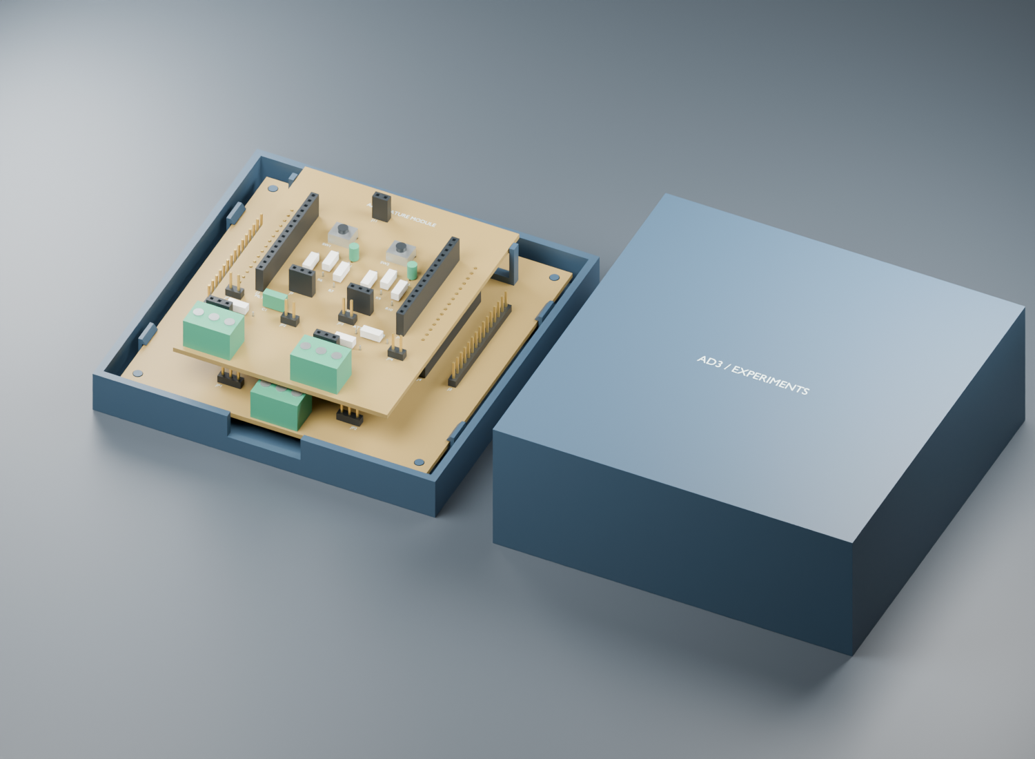
The plug-in configuration adds a low-pass filter, attenuator, selectable loopback paths, signal terminals, two buttons and two LEDs. Remove the breadboard before fitting the module. See the module assembly and test guide for wiring, soldering and AD3 commissioning.
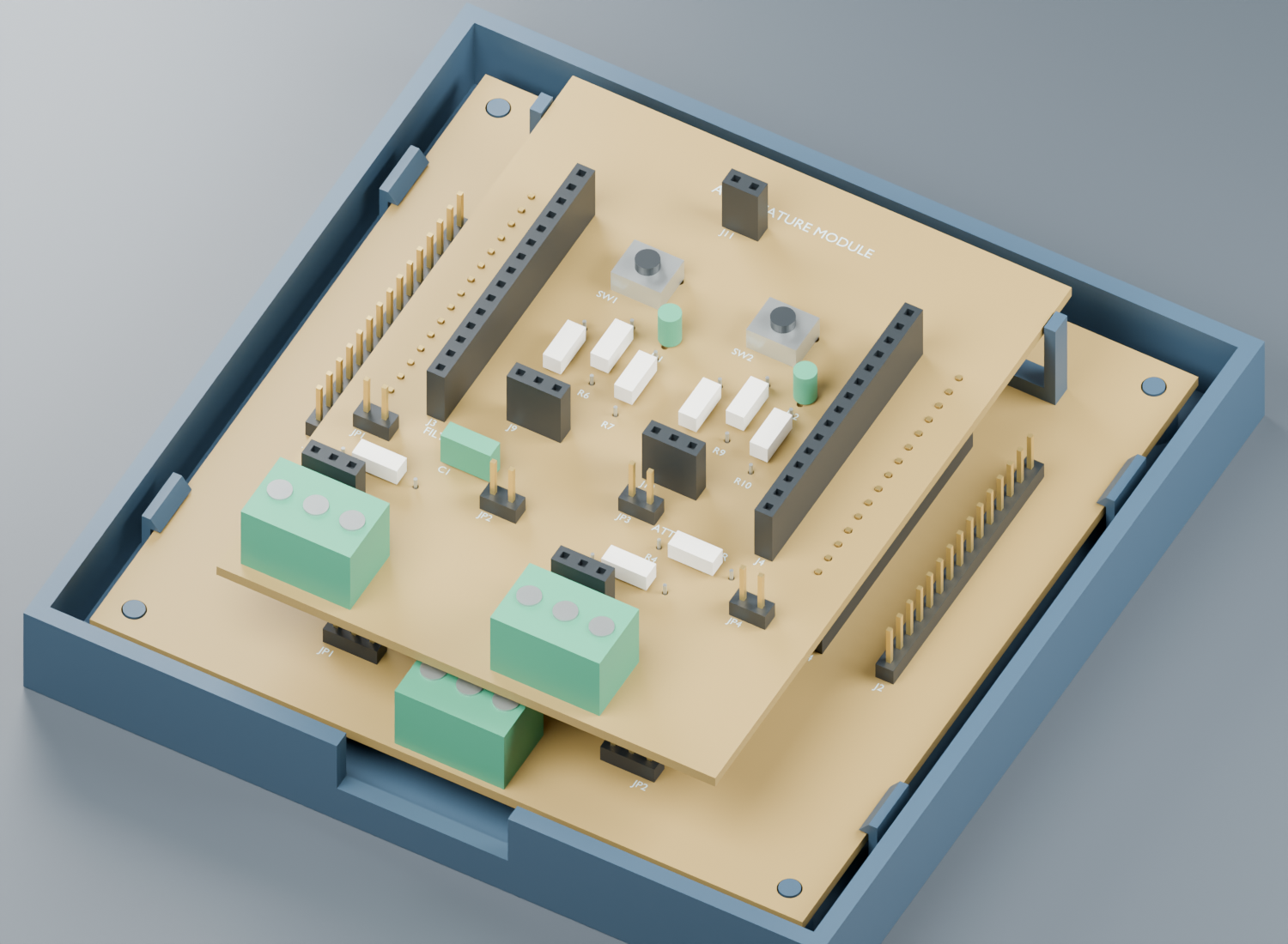
The module uses a printed support and taller storage cover. Download the Blender assembly, support STL and tall cover STL.
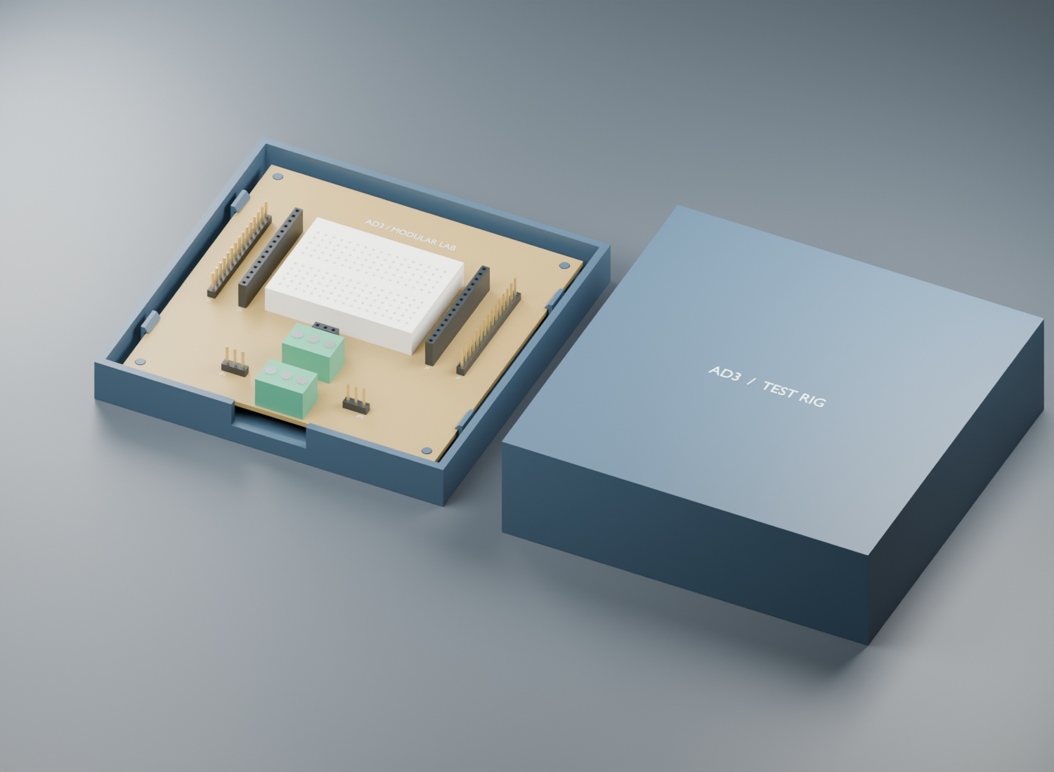
The original breadboard configuration remains available. These are design renders with illustrative component bodies; physical hardware and first-print fit have not yet been verified.
Open hardware/ad3-test-rig.kicad_pro in KiCad 10. Start the showcase with python serve.py, then visit http://localhost:8081.
hardware/: schematic, routed board, project-local footprint library and rules.hardware/production/: unmirrored B.Cu Gerber, outline, silkscreen and drill data.enclosure/: Blender source, editable scene, base/cover STLs and assembly GLB.website/: local showcase, interactive pinout, model inspection and assembly checklist.bench/: commissioning procedure and opt-in WaveForms SDK loopback test.tests/: generated electrical, inventory and mechanical reports.J1/J2 are male 15-pin banks for the individual female flywires. J3/J4 are matching female sockets, 60 mm between bank centre lines, for patching or a future module. Pins 1–15 run toward increasing PCB Y. All four grounds are common. CH1− and CH2− remain independent differential inputs. The AD3's positive and negative supplies pass straight to J3/J4 pin 4.
J5 is bench input (+, GND, −), J6 is selected-power screw terminal and J7 a selected-power module socket. JP1/JP2 choose AD3 (1–2), bench (2–3), or disconnected (no shunt). The selected rails do not replace raw supplies on J3/J4. A future module can ignore bank pin 4 and use J7 if it needs selected power. A module and the breadboard may occupy the same central space; remove the breadboard before fitting a full-width module. The optional feature module is now included in module/: a separate 70 × 90 mm KiCad project with analog experiments, buttons, LEDs, a printed support and taller cover. See module instructions.
B.Cu tracks are 1.0 mm wide; global copper clearance is 0.85 mm. Header pads were narrowed to 1.6 mm with 1.0 mm drills: their 2.54 mm pitch leaves 0.94 mm copper clearance. All joints are soldered from the bottom; no vias, top tracks, plated-through connectivity or wire bridges. Through-hole pads appear on both KiCad copper layers, but only bottom copper is fabricated. No mask is needed. If the blank has copper on both sides, remove the unused top copper rather than leaving it shorting the component leads.
The 100 × 100 mm finished outline assumes stock large enough for fixturing and an outline cut; a blank exactly that size cannot provide sacrificial edge stock. CAM must use the actual tool and machine settings. A nominal 0.8 mm cutter has only 0.05 mm total margin against the 0.85 mm rule. Verify tool runout and a small milling coupon before the board. Gerbers are not machine-ready motion programs; perform the bottom-view mirroring once in CAM/fixturing, not in these files.
The shop CSV names generic parts, not manufacturers or exact mechanical sizes. Assumptions to check before milling: headers 2.54 mm pitch; terminal blocks 5.08 mm pitch with pin/housing geometry fitting the vendored Phoenix-style footprint. No claim of measured fit or actual shelf quantity is made. The breadboard, existing AD3 cable, patch wires, PCB blank and print filament are user-selected equipment/fabrication supplies; the breadboard is not listed in the CSV. No extra purchased fasteners are needed.
PETG suggested for the four flexible retention fingers; 0.2 mm layers, at least 3 perimeters. Base 112 × 112 × 14 mm; cover 117.6 × 117.6 × 34.4 mm. STLs are millimetres and already oriented with their solid floor/roof on the build plate. Verify slicer dimensions. The PCB rests at Z=8.4 mm, leaving 6 mm above the inside floor for solder tails. Trim tails below 3 mm. A front-wall notch clears the bench terminal wiring. Four 2.8 mm printed locating pins enter the 3.2 mm PCB holes; snap fingers retain the edges with 0.4 mm nominal clearance above a 1.6 mm board. Cover is for storage with all cables removed. First-print mechanical fit remains untested; tune clip and cover clearances to your printer. The Blender component bodies and breadboard are illustrative, not manufacturer-certified CAD models.
Python 3.14 with KiCad's pcbnew and sexpdata, KiCad 10, Blender 5.2 and numpy for bench analysis were used. scripts/build.py uses the local schematic drawing toolkit at /home/mads/Projects/claude-skills/kicad-schematic/scripts; set that path in the script on another machine. Generated KiCad files are standalone and do not need the toolkit to open or edit. Run scripts/build.py only to regenerate from its design specification; it overwrites generated hardware files. After hand edits in KiCad, export and validate without regenerating. python scripts/export.py refreshes ERC/DRC, schematic PDF and fabrication exports after edits. python tests/verify.py verifies inventory, pinout, copper-layer constraints, print meshes and loopback fault rejection. scripts/geometry.py refreshes layout data for blender -b --python enclosure/build_enclosure.py.
Pinout and instrument reference: Digilent AD3 guide. The included pinout image comes from the installed Digilent WaveForms documentation. Stock footprints derive from KiCad libraries (CC-BY-SA 4.0 with library exception).
The baseboard schematic, copper and outline are unchanged. The new module replaces the breadboard while fitted, retains all AD3 signals on top sockets, and provides patchable filter/attenuator/loopback and digital test sections. Its purchased components also match the original shop CSV, with exact category matching for ambiguous part names. Use the dark-mode showcase for module placement, resistor colour codes and jumper states. Module hardware and first-print fit remain unverified; digital and analog commissioning instructions and SDK scripts are in module/.
| Qty | Value | Footprint | References |
|---|---|---|---|
| 5 | 1k | Module:resistor | R1, R6, R7, R9, R10 |
| 3 | 10k | Module:resistor | R4, R5, R8 |
| 2 | 3V3 BTN LED | Module:female3 | J9, J10 |
| 2 | ACTIVE LOW | Module:button | SW1, SW2 |
| 2 | BYPASS | Module:male2 | JP1, JP3 |
| 2 | GREEN | Module:led | D1, D2 |
| 2 | SHUNT ENABLE | Module:male2 | JP2, JP4 |
| 1 | 100k | Module:resistor | R3 |
| 1 | 100n | Module:capacitor | C1 |
| 1 | ATTEN IN OUT GND | Module:term3 | J6 |
| 1 | ATTEN PATCH | Module:female3 | J8 |
| 1 | BASE A / UNDERSIDE | Module:male15 | J1 |
| 1 | BASE B / UNDERSIDE | Module:male15 | J2 |
| 1 | EXTERNAL 3.3 V ONLY | Module:female2 | J11 |
| 1 | FILTER IN OUT GND | Module:term3 | J5 |
| 1 | FILTER PATCH | Module:female3 | J7 |
| 1 | PATCH A | Module:female15 | J3 |
| 1 | PATCH B | Module:female15 | J4 |
MadsRudolph/ad3-test-rig
CNC-friendly Analog Discovery 3 test rig with a plug-in experiment board, printable enclosure and assembly guide

gusmanb/logicanalyzer
24 channel, 100Msps logic analyzer hardware and software

VoronDesign/Voron-Hardware
Cool Hardware designed by the Voron Design group

hoglet67/RGBtoHDMI
Bare-metal Raspberry Pi project that provides pixel-perfect sampling of Retro Computer RGB/YUV video and conversion to HDMI

hackclub/OnBoard
💡 Join 1,000 teenagers and make your first PCB with a $100 grant!

OLIMEX/DIY-LAPTOP
Do It Yourself Open Source Hardware and Software Modular Hacker's Friendly Laptop

UtilitechAS/amsreader-firmware
ESP8266 and ESP32 compatible firmware to read, interpret and publish data to MQTT from smart electrical meters, both DLMS and DSMR is supported


It measures 70 × 90 mm and has 2 copper layers, 1.6 mm thick.
29 parts. The full list of its parts is on this page, with links to each part's symbol and footprint where PCBKit's library has them.
From the MadsRudolph/ad3-test-rig repository on GitHub, at the commit this page was made from: the board is module/hardware/ad3-feature-module.kicad_pcb and its schematic hardware/ad3-test-rig.kicad_sch. PCBKit opens the board in the browser, with nothing to install.
Its repository states no licence, so its author keeps all rights: ask MadsRudolph before reusing the design.