2 layers144.9 × 125.3 mm
Daughterboard (Cantaloupe)
Kaleidogeist/Galia
Modular split ergonomic keyboard system
53 partsCERN-OHL-S-2.0

 Kaleidogeist/Galia
Modular split ergonomic keyboard system
Motherboard (G0B1) is an open-source printed circuit board by Kaleidogeist, from the Kaleidogeist/Galia repository on GitHub, published under the CERN-OHL-S-2.0 licence. It is a 4-layer board of 50 × 32 mm with 68 parts on 82 nets, routed with 401 tracks and 109 vias.
It is built around the STM32G0B1CCU7, TPD4E05U06QDQARQ1 and TPS2553DRVR-1, with the XC6206P332MR-G, ESD321DPYR and CL05B104KB54PNC among its other parts. Its parts include 20 resistors, 13 diodes, 12 capacitors, 6 ICs and 4 connectors. It belongs with the computers and single-board computers boards and the STM32 boards of this library.


Modular split ergonomic keyboard system with each half consisting of a central motherboard and a hot-swappable key cluster daughterboard to allow for maximum flexibility.
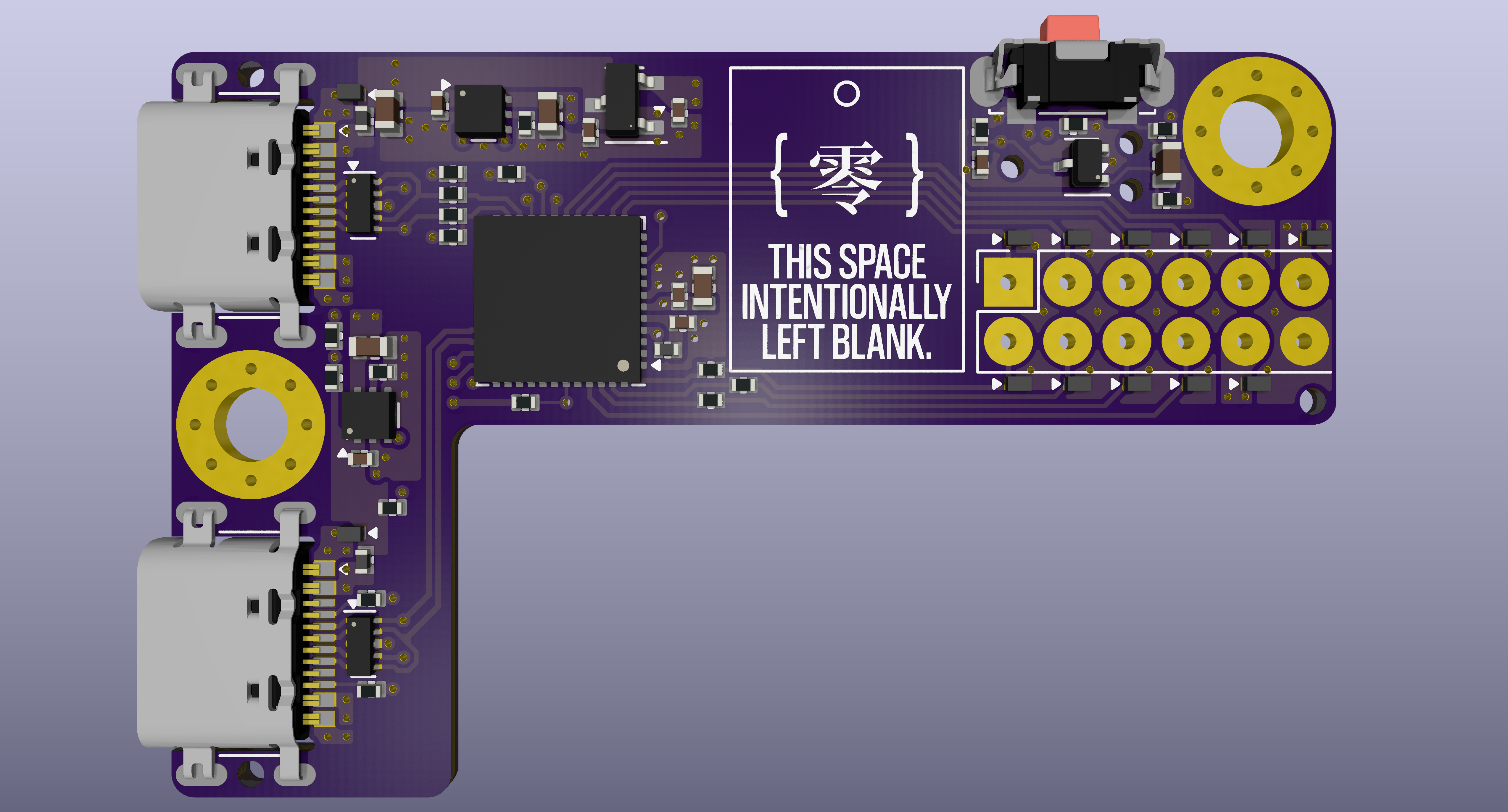
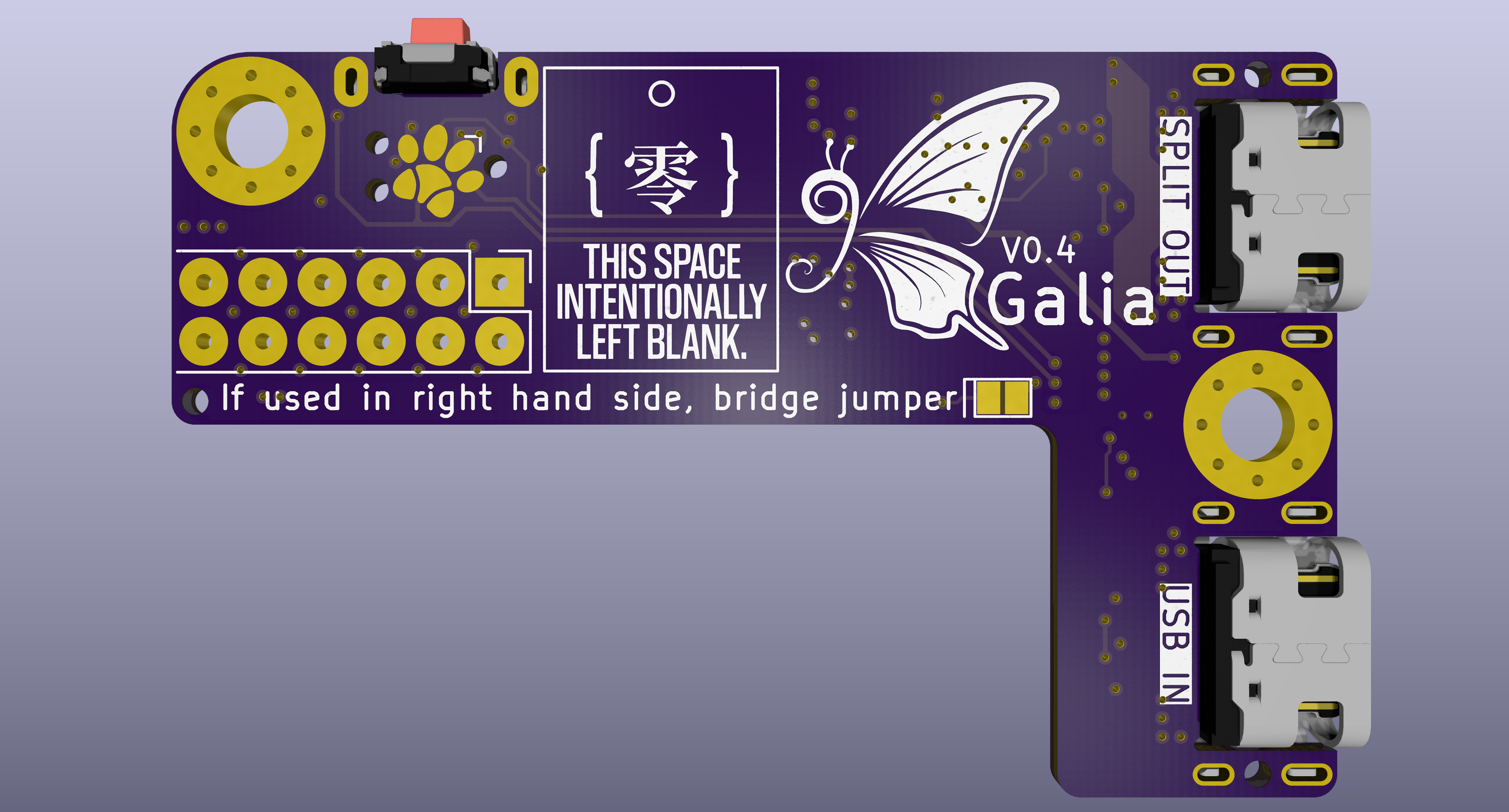
Current version: N/A (wip).
This keyboard is licensed under CERN-OHL-S-2.0 and is compatible with both QMK Firmware and ZMK Firmware.
| Function/description | Pin name | Row 1 | Row 2 | Pin name | Function/description |
|---|---|---|---|---|---|
| USART2_TX/ADC1_IN2/TIM2_CH3 | A2 | GPIO1 | CS | B9 | SPI2_NSS/I2C1_SDA/USART3_RX/TIM4_CH4 |
| USART2_RX/ADC1_IN3/TIM2_CH4 | A3 | GPIO2 | SCK | B8 | SPI2_SCK/I2C1_SCL/USART3_TX/TIM4_CH3 |
| SPI1_SCK/ADC1_IN5/TIM2_CH1 | A5 | GPIO3 | MOSI | B7 | SPI2_MOSI/I2C1_SDA/USART1_RX/TIM4_CH2 |
| SPI1_MISO/ADC1_IN6/I2C2_SDA/TIM3_CH1 | A6 | GPIO4 | MISO | B6 | SPI2_MISO/I2C1_SCL/USART1_TX/TIM1_CH3 |
| SPI1_MOSI/ADC1_IN7/I2C2_SCL/TIM3_CH2 | A7 | GPIO5 | +5V | N/A | ~207mA max draw by daughterboard |
| 200mA max draw by this side overall | N/A | VDD | GND | A7 | GND |
| Qty | Value | Footprint | References |
|---|---|---|---|
| 10 | ESD321 | Kaleidogeist-Package:X1SON_0.6x1mm_P0.65mm_Texas_DPY0002A | D3, D4, D5, D6, D7, D8, D10, D11, D12, D13 |
| 5 | 10u | Kaleidogeist-Device:C_0603_1608Metric | C2, C5, C9, C11, C12 |
| 5 | 22 | Kaleidogeist-Device:R_0402_1005Metric | R22, R23, R24, R25, R26 |
| 4 | 100k | Kaleidogeist-Device:R_0402_1005Metric | R4, R7, R12, R18 |
| 4 | 100n | Kaleidogeist-Device:C_0402_1005Metric | C1, C3, C4, C8 |
| 4 | 5k1 | Kaleidogeist-Device:R_0402_1005Metric | R2, R3, R15, R16 |
| 3 | 10k | Kaleidogeist-Device:R_0402_1005Metric | R6, R9, R11 |
| 3 | 120@100 | Kaleidogeist-Device:L_0402_1005Metric | FB1, FB2, FB3 |
| 3 | 150k | Kaleidogeist-Device:R_0402_1005Metric | R5, R10, R19 |
| 3 | 1u | Kaleidogeist-Device:C_0402_1005Metric | C6, C7, C10 |
| 3 | ESD441 | Kaleidogeist-Package:X1SON_0.6x1mm_P0.65mm_Texas_DPY0002A | D1, D2, D9 |
| 3 | Tooling Hole | Kaleidogeist-HolePad:MountingHole_JLC-Tooling | TOOL1, TOOL2, TOOL3 |
| 2 | M3 | Kaleidogeist-HolePad:MountingHole_3.2mm_M3_Pad_Via | H1, H2 |
| 2 | TPD4E05U06 | Kaleidogeist-Package:USON-10_2.5x1.0mm_P0.5mm | U1, U6 |
| 2 | TPS2553-1 | Kaleidogeist-Package:WSON-6-1EP_2x2mm_P0.65mm_EP1x1.6mm | U3, U5 |
| 2 | This_Space_Intentionally_Left_Blank | Kaleidogeist-Logo:This_Space_Intentionally_Left_Blank | G***, G*** |
| 1 | 2N7002W | Kaleidogeist-Package:SOT-323_SC-70-3 | Q1 |
| 1 | 56k | Kaleidogeist-Device:R_0402_1005Metric | R8 |
| 1 | Pogo | Kaleidogeist-Header:PinHeader_2x06_2.54mm_MillMax_PogoTarget_419-10-212-00-001000-Double_Sided | J3 |
| 1 | Reset | Kaleidogeist-Switch:SW_Alps_SKSNLM_SKSNLP | SW1 |
| 1 | SPLIT_HAND_R | Kaleidogeist-Misc:SolderJumper-2_P1.2mm_Open_Pad1.0x1.4mm | JP1 |
| 1 | STM32G0B1CCU7 | Kaleidogeist-Package:QFN-48-1EP_7x7mm_P0.5mm_EP5.6x5.6mm | U2 |
| 1 | SWD | Paw-Connect:Paw-Connect_RevB_TC2030-IDC-NL_2x03_P1.27mm_Vertical | J4 |
| 1 | USB-C In | Kaleidogeist-Connector:USB_C_Receptacle_Molex_2169900001 | J1 |
| 1 | USB-C Split | Kaleidogeist-Connector:USB_C_Receptacle_Molex_2169900001 | J2 |
| 1 | XC6206P332MR | Kaleidogeist-Package:SOT-23-3 | U4 |
Kaleidogeist/Galia
Modular split ergonomic keyboard system


RockyMtnWolf/PY32-BQ25798-SolarCap-Charger
Solar MPPT supercapacitor charger: PY32F003 + TI BQ25798. KiCad hardware (core board + test baseboard) and firmware with UART AT-command runtime configuration.


Galacs/esp32s3-poc-devboard
ESP32-S3 based PoC board made to test step-down power supply design, 24v level shifter, crystal circuits and RF circuit

jackw01/scanlight
A better light source for scanning color negative film

s-t-e-f-a-n/twinusb
H₂H³ | Twin USB Host Switch × Triple USB Hub (with OLED Telemetry)

GeniePod/genie-hardware
GeniePod Home V1 hardware: MVP testing build, wiring, BOM, and planned interface-board/enclosure docs.
It measures 50 × 32 mm and has 4 copper layers, 1.04 mm thick.
68 parts, built around the STM32G0B1CCU7, TPD4E05U06QDQARQ1, TPS2553DRVR-1 and XC6206P332MR-G. The full list of its parts is on this page, with links to each part's symbol and footprint where PCBKit's library has them.
From the Kaleidogeist/Galia repository on GitHub, at the commit this page was made from: the board is Motherboard (G0B1)/Motherboard (G0B1).kicad_pcb and its schematic Daughterboard (Cantaloupe)/Daughterboard (Cantaloupe).kicad_sch. PCBKit opens the board in the browser, with nothing to install.
Its repository publishes it under the CERN-OHL-S-2.0 licence: you may reuse it on that licence's terms (keep the author's notice, and for a copyleft licence share your changes alike).