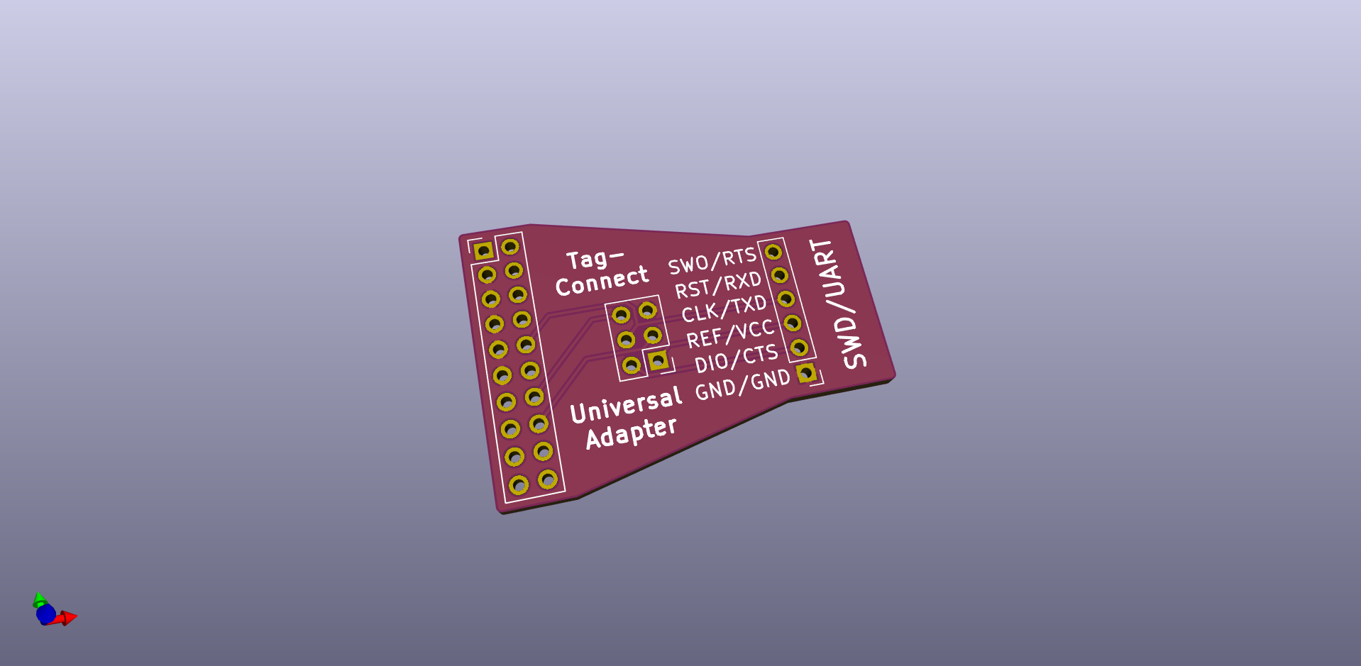
2 layers38.5 × 27 mm

 Jana-Marie/JlinkBreakout6
Segger Jlink to Tag-Connect and SWD adapter
JlinkBreakout is an open-source printed circuit board by Jana-Marie, from the Jana-Marie/JlinkBreakout repository on GitHub. It is a 2-layer board of 38.5 × 27 mm with 11 parts on 22 nets, routed with 87 tracks and 30 vias.
Its parts include 4 resistors, 3 connectors, 2 capacitors and 2 ICs. It belongs with the interfaces and adapters boards of this library.
Segger Jlink to Tag-Connect/SWD breakout board.
Notes:
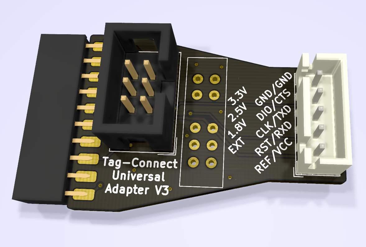
| Qty | Value | Footprint | References |
|---|---|---|---|
| 2 | 1u | Capacitor_SMD:C_0805_2012Metric | C1, C2 |
| 1 | 10.8k | Resistor_SMD:R_0603_1608Metric | R3 |
| 1 | 10k | Resistor_SMD:R_0603_1608Metric | R1 |
| 1 | 17.5k | Resistor_SMD:R_0603_1608Metric | R2 |
| 1 | 5k | Resistor_SMD:R_0603_1608Metric | R4 |
| 1 | JLINK | otter:conn_02x10_edge | J1 |
| 1 | SGM2019 | Package_TO_SOT_SMD:SOT-23-5 | U1 |
| 1 | SWD | Connector_JST:JST_XH_B5B-XH-A_1x05_P2.50mm_Vertical | J3 |
| 1 | TC | Connector_IDC:IDC-Header_2x03_P2.54mm_Vertical | J2 |
| 1 | switch_0204 | otter:SS-24E06-TG | U2 |

google/mozc-devices
Circuit diagrams and firmware source code for Gboard DIY keyboards


FrameworkComputer/ExpansionCards
Reference designs and documentation to create Expansion Cards for the Framework Laptop

hoglet67/RGBtoHDMI
Bare-metal Raspberry Pi project that provides pixel-perfect sampling of Retro Computer RGB/YUV video and conversion to HDMI

hackclub/OnBoard
💡 Join 1,000 teenagers and make your first PCB with a $100 grant!


tardate/LittleArduinoProjects
a collection of "Little Electronic & Arduino Projects", most involving electronics or an Arduino in one way or another!

basilfx/TRADFRI-Hacking
Hacking IKEA TRÅDFRI products, such as light bulbs, window blinds and other accessories.
It measures 38.5 × 27 mm and has 2 copper layers, 1.6 mm thick.
11 parts. The full list of its parts is on this page, with links to each part's symbol and footprint where PCBKit's library has them.
From the Jana-Marie/JlinkBreakout repository on GitHub, at the commit this page was made from: the board is V3/JlinkBreakout.kicad_pcb. PCBKit opens the board in the browser, with nothing to install.
Its repository states no licence, so its author keeps all rights: ask Jana-Marie before reusing the design.