6 layers30.5 × 18 mm

 HarmonInstruments/JTAG_SWD5
A USB to JTAG and SWD adapter for use with OpenOCD
USB JTAG is an open-source printed circuit board by HarmonInstruments, from the HarmonInstruments/JTAG_SWD repository on GitHub, published under the GPL-3.0 licence. It is a 4-layer board of 33.5 × 15 mm with 29 parts on 45 nets, routed with 216 tracks and 42 vias.
Its parts include 9 capacitors, 9 resistors, 7 ICs and 2 connectors. It belongs with the interfaces and adapters boards of this library.
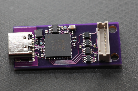
Hirose DF3A-6P-2DS header
Hirose DF3-6EP-2C 6 pin inline header
TC2030-MCP TC2030-MCP-NL
| Pin | JTAG | Serial Wire | AVR |
|---|---|---|---|
| 1 | VCC | VCC | VCC |
| 2 | TCK | SWCLK | SCK |
| 3 | GND | GND | GND |
| 4 | TDO | SWDIO | MISO |
| 5 | NC | jumper to 6 | NC |
| 6 | NC | jumper to 5 | NC |
| 7 | TDI | SWDIO | MOSI |
| 8 | TMS | NC | RST |
interface ftdi
ftdi_channel 0
ftdi_vid_pid 0x0403 0x6014
ftdi_layout_init 0x0058 0x00fb
ftdi_layout_signal nTRST -data 0x0010
ftdi_layout_signal nSRST -oe 0x0020
adapter_khz 10000

telnet_port 4444
gdb_port 3333
transport select jtag
reset_config none

jtag newtap lfe5 tap -expected-id 0x21111043 -irlen 8 -irmask 0xFF -ircapture 0x5
init
scan_chain
svf -tap lfe5.tap -quiet -progress build/display_fpga.svf
shutdowninterface ftdi
ftdi_channel 0
ftdi_vid_pid 0x0403 0x6014
ftdi_layout_init 0x0058 0x00fb
ftdi_layout_signal nTRST -data 0x0010
ftdi_layout_signal nSRST -oe 0x0020
telnet_port 4444
gdb_port 3333
transport select jtag
reset_config none
jtag newtap artix7 tap -irlen 6 -ignore-version -expected-id 0x0362E093
pld device virtex2 artix7.tap
adapter_khz 10000
adapter_nsrst_delay 200
init
pld load 0 top.bit
virtex2 read_stat 0
shutdownswd.cfg
source [find openocd.cfg]
flash info 0
flash write_image erase digital.elf
reset run
exit
openocd.cfg
interface ftdi
transport select swd
ftdi_channel 0
ftdi_vid_pid 0x0403 0x6014
ftdi_layout_init 0x0058 0x00fb
ftdi_layout_signal SWD_EN -data 0x0200
adapter_khz 1000
telnet_port 4444
gdb_port 3333
reset_config none
source [find target/stm32f4x.cfg]
init
reset halt
sleep 100avrdude -c c232hm -P USB -p m32u4 -v -b 500000Higher baud rates failed.
| Qty | Value | Footprint | References |
|---|---|---|---|
| 4 | 1 uF | kicad_pcb:C_0402_1005Metric | C1, C2, C3, C5 |
| 4 | 100 nF | kicad_pcb:C_0402_1005Metric | C6, C7, C9, C10 |
| 4 | 6MMF7 | kicad_pcb:SOT-363_SC-70-6 | U4, U5, U6, U8 |
| 3 | 12 k | kicad_pcb:R_0402_1005Metric | R2, R3, R4 |
| 2 | 499 | kicad_pcb:R_0402_1005Metric | R8, R9 |
| 2 | 5.1 k | kicad_pcb:R_0402_1005Metric | R6, R7 |
| 2 | tooling_hole | kicad_pcb:tooling_hole_2.55 | TH1, TH2 |
| 1 | 1 k | kicad_pcb:R_0402_1005Metric | R1 |
| 1 | 10 uF | kicad_pcb:C_0805_2012Metric | C4 |
| 1 | 26HRB | kicad_pcb:QFN-48-1EP_8x8mm_P0.5mm_EP6.2x6.2mm | U3 |
| 1 | 33 | kicad_pcb:R_0402_1005Metric | R5 |
| 1 | CGH8B | kicad_pcb:USB_C_Receptacle_HRO_TYPE-C-31-M-12 | J1 |
| 1 | Conn_01x08_Male | Connector_Hirose:Hirose_DF13-08P-1.25DSA_1x08_P1.25mm_Vertical | J2 |
| 1 | JPPQ9 | kicad_pcb:Oscillator_SMD_4Pin_2.5x2.0mm | U2 |
| 1 | Q6CVQ | kicad_pcb:SOT-23-6 | U1 |

Hanqaqa/Easyduino
Easily dive into different PCB KiCad designs of the most popular microcontroller devboards


EvanKrall/pipad
A PCB for putting a Raspberry Pi CM4 inside a 1st-generation iPad.


alvarop/chaac
This is a work in progress for a wireless weather station project.


colinleroy/BurgerDisk
A daisy-chainable Smartport hard drive for the Apple II

esden/glasgow-addons
Various interface addon boards and expansions for the Glasgow Digital Interface Explorer
It measures 33.5 × 15 mm and has 4 copper layers, 1.6 mm thick.
29 parts. The full list of its parts is on this page, with links to each part's symbol and footprint where PCBKit's library has them.
From the HarmonInstruments/JTAG_SWD repository on GitHub, at the commit this page was made from: the board is pcb/USB_JTAG.kicad_pcb and its schematic swd/USB_SWD.kicad_sch. PCBKit opens the board in the browser, with nothing to install.
Its repository publishes it under the GPL-3.0 licence: you may reuse it on that licence's terms (keep the author's notice, and for a copyleft licence share your changes alike).