2 layers32.5 × 57.5 mm
Schnupperblinki
GerritMihu/PCB-Production-with-Laser
Leiterplattenfertigung per Laser-Ablation (xTool F2 Ultra, Trotec Speedy) – Doku DE/EN, KiCad-Template, KiBot-Export
20 partsCC-BY-SA-4.0

 GerritMihu/PCB-Production-with-Laser
Leiterplattenfertigung per Laser-Ablation (xTool F2 Ultra, Trotec Speedy) – Doku DE/EN, KiCad-Template, KiBot-Export
Testlayout is an open-source printed circuit board by GerritMihu, from the GerritMihu/PCB-Production-with-Laser repository on GitHub, published under the CC-BY-SA-4.0 licence. It is a 2-layer board of 100 × 80 mm with 34 parts on 18 nets, routed with 79 tracks and 0 vias.
🇩🇪 Deutsch · ← Overview
Standardised test board (100 × 80 mm, single-sided F.Cu) for comparing fabrication methods under identical conditions:
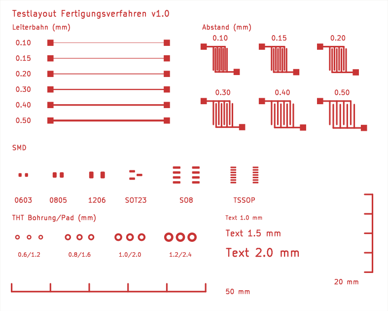
| Field | Content | Check |
|---|---|---|
| Track width | Tracks 0.10 / 0.15 / 0.20 / 0.30 / 0.40 / 0.50 mm, 30 mm long between two test pads | Continuity and resistance (multimeter), width under magnifier/microscope |
| Clearance | Comb structures with gaps 0.10 … 0.50 mm (track width 0.4 mm) | Isolation between pad A and pad B (multimeter: no continuity) |
| SMD | 0603, 0805, 1206, SOT-23, SOIC-8, TSSOP-14 (KiCad standard library) | Pads complete and separated? Test assembly |
| THT | Drill/pad 0.6/1.2 · 0.8/1.6 · 1.0/2.0 · 1.2/2.4 mm | Annular ring after drilling, alignment |
| Text | Copper text 1.0 / 1.5 / 2.0 mm | Legibility |
| Scale | 50 mm (X) and 20 mm (Y) with ticks | Dimensional accuracy with calipers |
The template's design rules are deliberately lowered for this project (min. 0.1 mm) so the test structures pass DRC. Normal projects keep the values from design rules.
See the German version README.de.md for the full procedure and the measurement sheet.
generate_testlayout.py creates testlayout.kicad_pcb and testlayout.kicad_pro (values editable at the top of the script). Open in KiCad and run DRC afterwards.laser/.| Qty | Value | Footprint | References |
|---|---|---|---|
| 24 | Testpad | Testlayout:Testpad_1.6mm | TP1, TP2, TP10, TP11, TP12, TP13, TP14, TP15, TP16, TP17, TP18, TP19, TP20, TP21, TP22, TP23 +8 |
| 1 | Bohrung 0.6 / Pad 1.2 | Testlayout:THT_D0.6_P1.2 | H1 |
| 1 | Bohrung 0.8 / Pad 1.6 | Testlayout:THT_D0.8_P1.6 | H2 |
| 1 | Bohrung 1 / Pad 2 | Testlayout:THT_D1_P2 | H3 |
| 1 | Bohrung 1.2 / Pad 2.4 | Testlayout:THT_D1.2_P2.4 | H4 |
| 1 | R_0603_1608Metric | Resistor_SMD:R_0603_1608Metric | U1 |
| 1 | R_0805_2012Metric | Resistor_SMD:R_0805_2012Metric | U2 |
| 1 | R_1206_3216Metric | Resistor_SMD:R_1206_3216Metric | U3 |
| 1 | SOIC-8_3.9x4.9mm_P1.27mm | Package_SO:SOIC-8_3.9x4.9mm_P1.27mm | U5 |
| 1 | SOT-23 | Package_TO_SOT_SMD:SOT-23 | U4 |
| 1 | TSSOP-14_4.4x5mm_P0.65mm | Package_SO:TSSOP-14_4.4x5mm_P0.65mm | U6 |
GerritMihu/PCB-Production-with-Laser
Leiterplattenfertigung per Laser-Ablation (xTool F2 Ultra, Trotec Speedy) – Doku DE/EN, KiCad-Template, KiBot-Export


FrameworkComputer/ExpansionCards
Reference designs and documentation to create Expansion Cards for the Framework Laptop

mntmn/amiga2000-gfxcard
MNT VA2000, an Open Source Amiga 2/3/4000 Graphics Card (Zorro II/III), written in Verilog

hackclub/OnBoard
💡 Join 1,000 teenagers and make your first PCB with a $100 grant!


strangeparts/niubi-headphones
Flexible circuit board design for adding a headphone jack to an iPhone 7


baldengineer/bit-preserve
Project for capturing vintage, classic, aka old computer schematics in KiCad.
It measures 100 × 80 mm and has 2 copper layers, 1.6 mm thick.
34 parts. The full list of its parts is on this page, with links to each part's symbol and footprint where PCBKit's library has them.
From the GerritMihu/PCB-Production-with-Laser repository on GitHub, at the commit this page was made from: the board is examples/testlayout/testlayout.kicad_pcb and its schematic examples/schnupperblinki/schnupperblinki.kicad_sch. PCBKit opens the board in the browser, with nothing to install.
Its repository publishes it under the CC-BY-SA-4.0 licence: you may reuse it on that licence's terms (keep the author's notice, and for a copyleft licence share your changes alike).