2 layers55.8 × 55.8 mm
ControlBoard
D3epCr3ature/RE-CPNV-ElectronicDice
Reverse engineering of an electronic dice assembled during my diploma of Vocational Education and Training (VET) in electronics.
27 parts

 GerritMihu/Mosfet-Halfbridge
Mosfet-Half-Bridge
Pushpull Highside Driver is an open-source printed circuit board by GerritMihu, from the GerritMihu/Mosfet-Halfbridge repository on GitHub. It is a 2-layer board of 63 × 46 mm with 35 parts on 19 nets, routed with 210 tracks and 0 vias.
It is built around the BC846, BC856 and IRFR120NTR, with the LL4148 among its other parts. Its parts include 15 resistors, 10 transistors, 5 capacitors, 3 connectors and 2 diodes.


Diskreter Halbbrücken-Treiber mit Bootstrap für 24 V, aufgebaut nur aus Kleinsignal-Transistoren.
KiCad-Projekt: Pushpull-Highside-Driver/
| Stecker | Pin | Funktion |
|---|---|---|
| J3 | 1 / 2 | +24 V / GND |
| J4 | 3 / 2 / 1 | HS_IN / LS_IN / GND (3,3-V- oder 5-V-Logik) |
| J1 | 1 / 2 | SW (Ausgang) / GND |
HIGH am Eingang schaltet den MOSFET ein, ein offener Eingang schaltet ihn aus.
HS_IN und LS_IN dürfen nie gleichzeitig HIGH sein. Der Controller muss die Totzeit erzeugen: In der Simulation schaltet der Treiber rund 1 µs langsamer aus als ein. Plane deshalb mit Reserve mindestens 2 µs ein; die Testquellen nutzen 3 µs. Vor dem ersten Highside-Puls muss die Lowside kurz einschalten, damit C2 (Bootstrap) geladen wird.
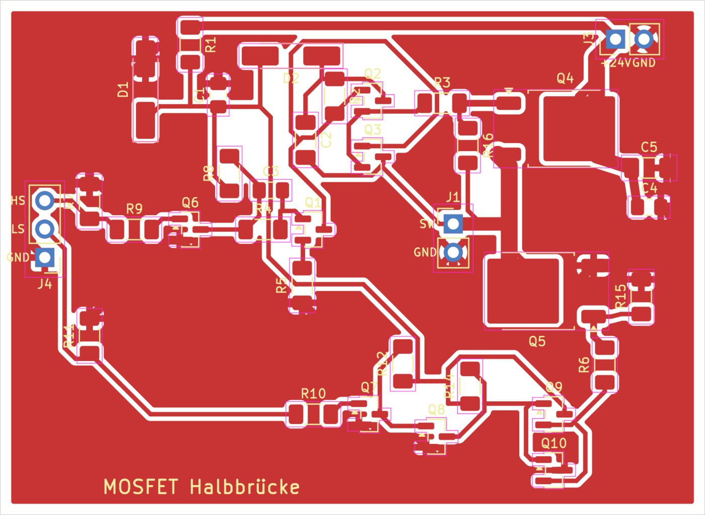
Einseitiges Layout (nur F.Cu, keine Vias, keine Brücken) für Laser-Ablation mit dem xTool F2 Ultra. Signalbahnen 0,4 mm, +24V/GND 0,8 mm, Abstand 0,2 mm, Randabstand 1 mm. Freie Flächen sind mit GND gefüllt.
| Netz (Bahnlänge) | erstes Layout | jetzt |
|---|---|---|
| Gate Q4 | 11,7 mm | 7,0 mm |
| Gate Q5 | 15,5 mm | 7,5 mm |
| Emitter Q2/Q3 → R3 | 16,4 mm | 11,9 mm |
| BOOT | 42,9 mm | 13,2 mm |
| Abstand C4/C5 zu Q4/Q5 | ca. 40 mm | ca. 3 mm |
| Vias/Drahtbrücken | 10 / 5 | 0 / 0 |
Im Schaltplan sind fertig eingerichtet: SPICE-Modelle (sim/halfbridge_models.lib),
Quellen V1–V3 und Last RL1 (24 Ω). Diese Teile kommen nicht auf die Platine und nicht in die Stückliste.
So startest du sie: Schaltplan öffnen → Prüfen → Simulator → Simulation starten → Signale wie SW, BOOT, HS_IN auswählen.
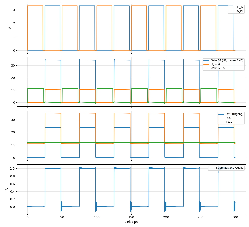
Bedingungen: 24 V, 20 kHz, 24 Ω Last, Eingänge 3,3 V.
| Größe | Simulation | Messung |
|---|---|---|
| SW High / Low | 23,8 V / ≈ 0 V | |
| Ugs Q4 (Highside) | ≈ 10,6 V | |
| Ugs Q5 (Lowside) | ≈ 11,9 V | |
| BOOT gegen GND (SW high) | ≈ 35 V | |
| +12-V-Schiene | 12,0 V | |
| Verzögerung HS_IN ↑ → SW 50 % | 0,24 µs | |
| Verzögerung HS_IN ↓ → SW 50 % | 1,2 µs | |
| Verzögerung LS_IN ↑ → Gate Q5 6 V | 0,24 µs | |
| Verzögerung LS_IN ↓ → Gate Q5 6 V | 1,2 µs | |
| SW-Anstieg 10–90 % | 0,05 µs |
Die Modelle sind Näherungen aus typischen Datenblattwerten. Spannungen sollten gut passen. Bei Zeiten sind Abweichungen zu erwarten, und Überschwingen durch Leiterbahn-Induktivität fehlt in der Simulation ganz – genau das lässt sich mit den Schülern gut diskutieren.
Messhinweis: Ugs von Q4 nur mit Differenztastkopf messen oder aus zwei Kanälen gegen GND berechnen. Die Oszilloskop-Masse liegt auf GND, nicht auf SW.
| Qty | Value | Footprint | References |
|---|---|---|---|
| 6 | 10k | Resistor_SMD:R_1206_3216Metric_Pad1.30x1.75mm_HandSolder | R7, R8, R11, R12, R15, R16 |
| 6 | BC846 | Package_TO_SOT_SMD:SOT-23 | Q1, Q2, Q6, Q7, Q8, Q9 |
| 3 | 2k2 | Resistor_SMD:R_1206_3216Metric_Pad1.30x1.75mm_HandSolder | R4, R9, R10 |
| 2 | 10R | Resistor_SMD:R_1206_3216Metric_Pad1.30x1.75mm_HandSolder | R3, R6 |
| 2 | 4k7 | Resistor_SMD:R_1206_3216Metric_Pad1.30x1.75mm_HandSolder | R2, R14 |
| 2 | BC856 | Package_TO_SOT_SMD:SOT-23 | Q3, Q10 |
| 2 | IRFR120N | Package_TO_SOT_SMD:TO-252-2 | Q4, Q5 |
| 1 | 100R | Resistor_SMD:R_1206_3216Metric_Pad1.30x1.75mm_HandSolder | R5 |
| 1 | 100n | Capacitor_SMD:C_1206_3216Metric_Pad1.33x1.80mm_HandSolder | C2 |
| 1 | 100n | Capacitor_SMD:C_0805_2012Metric_Pad1.18x1.45mm_HandSolder | C4 |
| 1 | 10u | Capacitor_SMD:C_1206_3216Metric_Pad1.33x1.80mm_HandSolder | C5 |
| 1 | 12V | Diode_SMD:D_MiniMELF_Handsoldering | D1 |
| 1 | 1k | Resistor_SMD:R_1206_3216Metric_Pad1.30x1.75mm_HandSolder | R1 |
| 1 | 1u | Capacitor_SMD:C_0805_2012Metric_Pad1.18x1.45mm_HandSolder | C1 |
| 1 | 220p | Capacitor_SMD:C_0805_2012Metric_Pad1.18x1.45mm_HandSolder | C3 |
| 1 | 24V Versorgung | Connector_PinHeader_2.54mm:PinHeader_1x02_P2.54mm_Vertical | J3 |
| 1 | Controller (GND, LS, HS) | Connector_PinHeader_2.54mm:PinHeader_1x03_P2.54mm_Vertical | J4 |
| 1 | LL4148 | Diode_SMD:D_MiniMELF_Handsoldering | D2 |
| 1 | Last | Connector_PinHeader_2.54mm:PinHeader_1x02_P2.54mm_Vertical | J1 |
D3epCr3ature/RE-CPNV-ElectronicDice
Reverse engineering of an electronic dice assembled during my diploma of Vocational Education and Training (VET) in electronics.


eilbek-research/er-schultzcontroller
G-code controller for Siemens S (Schultz) feeders

MG-5/vfd-clock-hardware
Hardware for controlling six VFD IV-17 tubes as clock (HH:MM:SS)

alexcrt12/p1-stabilizator-ers-orcad-schematic-kicad-layout
My Voltage regulator project, for which I have used OrCAD for the schematic and simulations and KiCad for the PCB layout


It measures 63 × 46 mm and has 2 copper layers, 1.6 mm thick.
35 parts, built around the BC846, BC856, IRFR120NTR and LL4148. The full list of its parts is on this page, with links to each part's symbol and footprint where PCBKit's library has them.
From the GerritMihu/Mosfet-Halfbridge repository on GitHub, at the commit this page was made from: the board is Pushpull-Highside-Driver/Pushpull-Highside-Driver.kicad_pcb and its schematic Pushpull-Highside-Driver/Pushpull-Highside-Driver.kicad_sch. PCBKit opens the board in the browser, with nothing to install.
Its repository states no licence, so its author keeps all rights: ask GerritMihu before reusing the design.